Download
1 / 13
170 likes | 548 Views
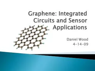
Graphene : Integrated Circuits and Sensor Applications. Daniel Wood 4-14-09. Talking Points. What is Graphene ? Historical Background How it is Made Applications Sensors Integrated Circuits Ending Thoughts

E N D
Graphene: Integrated Circuits and Sensor Applications Daniel Wood 4-14-09
Talking Points • What is Graphene? • Historical Background • How it is Made • Applications • Sensors • Integrated Circuits • Ending Thoughts “There is no doubt that graphene, a single layer of carbon atoms densely packed into a benzene-ring structure, is an excellent playground for condensed-matter physicists and MATERIALS SCIENTISTS.” – Novoselov and Geim(1)
What is Graphene • Is a 2D structure and 1 atom thick • Hexagonal array of sp2 carbon atoms. • Sigma orbital = valence band • Pi orbital = conduction band (2) • C-C bond is 120° and ~ 0.142nm bond length • Is electrically “metallic” 0D Buckyball(3) 1D CNT 3D Graphite
Historical Background • 1564 • Invention of the pencil in England (4) • 2004 (Oct 22) • I turned 20 • Novoselov and Geim publish “electric field effect in atomically thin carbon films” leading to development of graphene! • 2006 • Exponential explosion in research (350 publications) (1) • 2009 • Listening to this presentation
How its made • Drawing – mechanical exfoliation of 3D graphite crystals • Epitaxial growth – use of the atomic structure of substrate to grow graphene • Silicon Carbide Reduction – heating of silicon carbide to 1100C and reduce it to form graphene(5) • Other processes • Hydrazine Reduction • Sodium Reduction of Ethanol • CVD (4)
Applications • Transistors • Sensors • TEM • Inert Coatings • Nanoribbons and Semiconductors • Integrated circuits • Ultracapacitors • Biodevices(6)
Sensors • Purpose of Sensors • To have sensitivity to detect individual quanta of a certain entity ( i.e. ONE atom or molecule) • Current high sensitive sensors • CNT and semiconductor nanowires(7) • Upside = Cheap, small size, detect 1 p.p.b. • Downfall = noise greater than particle signal due to fluctuations in thermal motion of charges and defects. (8)
Sensors (cont…) • Why Graphene • How it works • Large changes in conductivity, σ , from gas adsorbates • Gas molecules act as donors or acceptors on graphene surface • Why it works • 1 : 2D entire surface is exposed to adsorbates • 2 : Exhibits metallic conductivity Low noise in limit of no charge carriers • 3 : Few crystal defects Low noise due to thermal motion • Upside = Sensitivity, No “poisoning” effects after annealing or UV cleaning • Downside = No graphene mass production techniques (8)
Integrated Circuits • Purpose of IC • Applied voltage to vary carrier concentration • Current IC • Use of Si as semiconductor • Upside = Works, Cheap, Industry standard • Downside = Cannot get much smaller or faster • Current non-traditional methods : organic conductors and CNT • Use of metals • Atomically thin films for ballistic transport • Thermodynamically unstable at small thickness (5)
Integrated Circuits (cont…) • Why Graphene • How it works • Why it works • Retain high carrier mobility with low resistance • High-quality transfer rate of graphene to substrates • Ability for different graphene/substrate geometeries • No exposure to chemical preparation • Upside = Sensitivity, low resistance, small, No “poisoning” effects from preparation • Downside = No graphene mass production techniques (5)
Ending Thoughts • What is Graphene: • Is a 2D structure and 1 atom thick • Hexagonal array of sp2 carbon atoms. • Is electrically “metallic” • 2004 was begining of research for graphene • How is it made? • Drawing, Epitaxial growth, Silicon Carbide Reduction • Why graphene? • Sensors, Integrated circuits, Transistors, TEM, Inert Coatings, Nanoribbons and Semiconductors, Ultracapacitors, Biodevices(6)
References • Graphene calling. Science. Vol.6. No.3. March 2007 • S banerjee, M. Sardar. Mapping conductivity of graphene sheets using conducting tip of AFM. Science-37 • A.K. Geim, K.S. Novoselov. The rise of graphene. Science Vol.6. March 2007. • http://en.wikipedia.org/wiki/Graphene • Jian-Hao Chen, MasaIshigami. Printed Graphene Circuits. Advanced Materials. 7007, 19, 3623-3627 • http://grapheneindustries.com/?What+is+graphene%3F • A.K. Geim, K.S. Novoselov. Electric Field Effect in Atomically Thin Carbon Films. Science. Vol 306. Oct 2004 • F. Schedin, A.K. Geim. Detection of individual gas molecules adsobed on graphene. Nature Materials. Vol.6. September 2007.