Download
1 / 31
490 likes | 1.03k Views
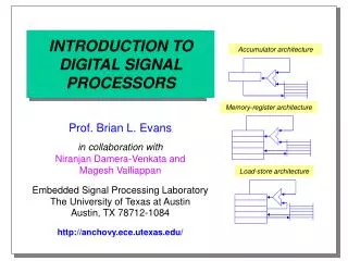
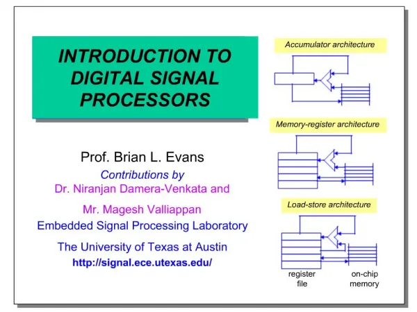
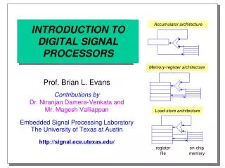
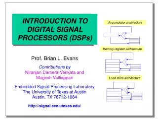
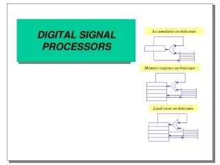
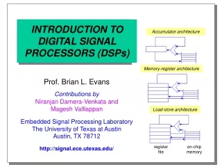
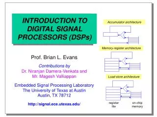
INTRODUCTION TO DIGITAL SIGNAL PROCESSORS (DSPs). Accumulator architecture. Memory-register architecture. Prof. Brian L. Evans Contributions by Dr. Niranjan Damera-Venkata and Mr. Magesh Valliappan Embedded Signal Processing Laboratory The University of Texas at Austin Austin, TX 78712

E N D
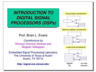
INTRODUCTION TODIGITAL SIGNALPROCESSORS (DSPs) Accumulator architecture Memory-register architecture Prof. Brian L. Evans Contributions byDr. Niranjan Damera-Venkata andMr. Magesh Valliappan Embedded Signal Processing LaboratoryThe University of Texas at AustinAustin, TX 78712 http://signal.ece.utexas.edu/ Load-store architecture register file on-chip memory
Outline • Signal processing applications • Conventional DSP architecture • Pipelining in DSP processors • RISC vs. DSP processor architectures • TI TMS320C6000 DSP architecture introduction • Signal processing on general-purpose processors • Conclusion
Signal Processing Applications • Embedded system demand: volume, volume, … • 400 Million units/year: automobiles, PCs, cell phones • 30 Million units/year: ADSL modems and printers • Consumer electronics products • How much should an embedded processor cost? Source: CEA Market Reseach (US). Data for 2004 calendar year.
Signal Processing Applications • Embedded system cost & input/output rates • Low-cost, low-throughput: sound cards, 2G cellphones, MP3 players, car audio, guitar effects • Medium-cost, medium-throughput: printers,disk drives, PDAs, 3G cell phones, ADSLmodems, digital cameras, video conferencing • High-cost, high-throughput: high-end printers,audio mixing boards, wireless basestations,high-end video conferencing, 3-D sonar,3-D medical reconstruction from 2-D X-rays • Embedded processor requirements • Inexpensive with small area and volume • Predictable input/output (I/O) rates to/from processor • Power constraints (severe for handheld devices) Single DSP Single DSP + Coprocessor Multiple DSPs
Conventional DSP Processors • Low cost: as low as $2/processor in volume • Deterministic interrupt service routine latency guarantees predictable input/output rates • On-chip direct memory access (DMA) controllers • Processes streaming input/output separately from CPU • Sends interrupt to CPU when block has been read/written • Ping-pong buffering • CPU reads/writes buffer 1 as DMA reads/writes buffer 2 • After DMA finishes buffer 2, roles of buffers 1 & 2 switch • Low power consumption: 10-100 mW • TI TMS320C54 0.32 mA/MIP 76.8 mW at 1.5 V, 160 MHz • TI TMS320C55 0.05 mA/MIP 22.5 mW at 1.5 V, 300 MHz • Based on conventional (pre-1996) architecture
Conventional DSP Architecture • Multiply-accumulate (MAC) in 1 instruction cycle • Harvard architecture for fast on-chip I/O • Data memory/bus separate from program memory/bus • One read from program memory per instruction cycle • Two reads/writes from/to data memory per inst. cycle • Instructions to keep pipeline (3-6 stages) full • Zero-overhead looping (one pipeline flush to set up) • Delayed branches • Special addressing modes supported in hardware • Bit-reversed addressing (e.g. fast Fourier transforms) • Modulo addressing for circular buffers (e.g. filters)
Data Shifting Using a Linear Buffer Time Buffer contents Next sample xN-K+1 xN-1 xN+1 xN-K+2 xN n=N xN-K+2 xN xN-K+3 xN+1 n=N+1 xN+2 xN-K+3 xN+1 xN-K+4 xN+2 n=N+2 xN+3 Conventional DSP Architecture (con’t) • Buffer of length K • Used in finite and infinite impulse response filters • Linear buffer • Sort by time index • Update: discard oldest data, copy old data left, insert new data • Circular buffer • Oldest data index • Update: insert new data at oldest index, update oldest index Modulo Addressing Using a Circular Buffer Time Next sample Buffer contents n=N xN-2 xN-K+1 xN xN+1 xN-1 xN-K+2 xN+2 xN-2 xN+1 xN xN xN-K+3 xN-1 xN-K+2 n=N+1 xN-2 xN+1 xN xN-1 xN xN+2 xN-K+3 xN-K+4 xN-K+4 n=N+2 xN+3
Conventional DSP Processor Families DSP Market (est.) Fixed-point 95%Floating-point 5% • Floating-point DSPs • Used in initial prototyping of algorithms • Resurgence in products due to professional and car audio • Different on-chip configurations in each family • Size and map of data and program memory • A/D, input/output buffers, interfaces, timers, and D/A • Drawbacks to conventional DSP processors • No byte addressing (needed for images and video) • Limited on-chip memory • Limited addressable memory on fixed-point DSPs (exceptions include Freescale 56300 and TI C5409) • Non-standard C extensions for fixed-point data type
Program RAM Data RAM or Cache Addr Internal Buses DMA Serial Port Host Port Boot Load Timers Pwr Down Data .D1 .D2 .M1 .M2 External Memory -Sync -Async Regs (A0-A15) Regs (B0-B15) .L1 .L2 .S1 .S2 Control Regs CPU Modern DSP Processor Family Texas Instruments TMS320C6000 DSP Simpilifed Architecture
TI TMS320C6000 DSP Architecture • Very long instruction word (VLIW) size of 256 bits • Eight 32-bit functional units with single cycle throughput • One instruction cycle per clock cycle • Data word size is 32 bits • 16 (32 on C6400) 32-bit registers in each of 2 data paths • 40 bits can be stored in adjacent even/odd registers • Two parallel data paths • Data unit - 32-bit address calculations (modulo, linear) • Multiplier unit - 16 bit 16 bit with 32-bit result • Logical unit - 40-bit (saturation) arithmetic & compares • Shifter unit - 32-bit integer ALU and 40-bit shifter
TI TMS320C6000 DSP Architecture • Families: All support same C6000 instruction set C6200 fixed-pt. 150- 300 MHz ADSL, printers C6400 fixed pt. 300-1,000 MHz video, wireless basestations C6700 floating 100- 300 MHz medical imaging, pro-audio • TMS320C6701 Evaluation Module (EVM) Board 200 MHz CPU (400 million MACs/s, 1600 RISC MIPS) On-chip memory: 16 kwords program, 16 kwords data On-board: one 133-MHz 64-kword, 2 100-MHz 1-Mword • TMS320C6713 DSP Starter Kit (DSK) Board 225 MHz CPU (450 million MACs/s, 1800 RISC MIPS) On-chip: 1 kword program, 1 kword data, 16 kword L2 On-board memory: 2-Mword SDRAM, 128 kword flash ROM
TI TMS320C6000 DSP Instruction Set C6000 Instruction Set by Functional Unit .S Unit ADD NEGADDK NOTADD2 ORAND SETB SHLCLR SHREXT SSHLMV SUBMVC SUB2MVK XORMVKH ZERO .L Unit ABS NOTADD ORAND SADDCMPEQ SATCMPGT SSUBCMPLT SUBLMBD SUBCMV XORNEG ZERONORM .D Unit ADD STADDA SUBLD SUBAMV ZERONEG .M Unit MPY SMPYMPYH SMPYH Other NOP IDLE Six of the eight functional units can perform integer add, subtract, and move operations
TI TMS320C6000 DSP Instruction Set ArithmeticABSADDADDAADDKADD2MPYMPYHNEGSMPYSMPYHSADDSATSSUBSUBSUBASUBCSUB2ZERO LogicalANDCMPEQCMPGTCMPLTNOTORSHLSHRSSHLXOR DataManagementLDMVMVCMVKMVKHST ProgramControlBIDLENOP BitManagementCLREXTLMBDNORMSET C6000 InstructionSet by Category (un)signed multiplicationsaturation/packed arithmetic
C6000 vs. C5000 Addressing Modes • Immediate • The operand is part of the instruction • Register • Operand is specified in a register • Direct • Address of operand is part of the instruction (added to imply memory page) • Indirect • Address of operand is stored in a register TI C5000 TI C6000 ADD #0FFh add .L1 -13,A1,A6 (implied) add .L1 A7,A6,A7 ADD 010h not supported ADD * ldw .D1 *A5++[8],A1
TI TMS320C6700 Extensions C6700 Floating Point Extensions by Unit .S Unit ABSDP CMPLTSP ABSSP RCPDPCMPEQDP RCPSP CMPEQSP RSARDP CMPGTDP RSQRSP CMPGTSP SPDPCMPLTDP .L Unit ADDDP INTSPADDSP SPINTDPINT SPTRUNCDPSP SUBDPDPTRUNC SUBSPINTDP .M Unit MPYDP MPYIDMPYI MPYSP .D Unit ADDAD LDDW Four functional units perform IEEE single-precision (SP) and double-precision (DP) floating-point add, subtract, and move. Operations beginning with R are reciprocal (i.e. 1/x) calculations.
Selected TMS320C6700 Floating-Point DSPs DSK means DSP Starter Kit. EVM means Evaluation Module. Unit price is for 1,000 units. Prices effective June 3, 2005. For more information:http://www.ti.com
Selected TMS320C6000 Fixed-Point DSPs C6416 has Viterbi and Turbo decoder coprocessors. Unit price is for 1,000 units. Prices effective June 3, 2005. For more information:http://www.ti.com
Pipelining Sequential(Freescale 56000) Fetch Decode Read Execute Pipelined(Most conventional DSPs) • Pipelining • Process instruction stream in stages (as stages of assembly on a manufacturing line) • Increase throughput • Managing Pipelines • Compiler or programmer • Pipeline interlocking Fetch Decode Read Execute Superscalar(Pentium) Fetch Decode Read Execute Superpipelined(TMS320C6000) Fetch Decode Read Execute
Fetch Decode Read Execute F D R E C D E F G H I J K - L D E F G H I J K L L B C D E F G H I J K - L A B C D E F G H I J K - L Pipelining: Operation • Time-stationary pipeline model • Programmer controls each cycle • Example: Freescale DSP56001 (has separate X/Y data memories/registers) • Data-stationary pipeline model • Programmer specifies data operations • Example: TI TMS320C30 • Interlocked pipeline • “Protection” from pipeline effects • May not be reported by simulators:inner loops may take extra cycles MAC X0,Y0,A X:(R0)+,X0 Y:(R4)-,Y0 MPYF *++AR0(1),*++AR1(IR0),R0 MAC means multiplication-accumulation.
Fetch Decode Read Execute F D R E D E F br G - - X Y Y Z CD E F br - - - X - Y Z BCD E F br - - - X - Y Z ABCD E F br - - - X - Y Z Pipelining: Control and Data Hazards • A control hazard occurs when a branch instruction is decoded • Processor “flushes” the pipeline, or • Use delayed branch (expose pipeline) • A data hazard occurs because an operand cannot be read yet • Intended by programmer, or • Interlock hardware inserts “bubble” • TI TMS320C5000 (20 CPU & 16 I/O registers, one accumulator, and one address pointer ARP implied by *) LAR AR2, ADDR ; load address reg. LACC *- ; load accumulator w/; contents of AR2 LAR: 2 cycles to update AR2 & ARP; need NOP after it
Pipelining: Avoiding Control Hazards Fetch Decode Read High throughput performance of DSPs is helped by on-chip dedicated logic for looping (downcounters/looping registers) • A repeat instruction repeats one instruction or a block of instructions after repeat • The pipeline is filled with repeated instruction (or block of instructions) • Cost: one pipeline flush only Execute F D R E D E F rpt X X X X X X X X C D E F rpt - - X X X X X B CD E F rpt - - X X X X ABCD E F rpt - - X X X ; repeat TBLR inst. COUNT-1 times RPT COUNT TBLR *+
TI TMS320C6000 DSP Pipeline Pentium IV pipelinehas more than 20 stages • C6000 has deep pipeline • 7-11 stages in C6200: fetch 4, decode 2, execute 1-5 • 7-16 stages in C6700: fetch 4, decode 2, execute 1-10 • Compiler and assembler must prevent pipeline hazards • Only branch instruction: delayed unconditional • Processor executes next 5 instructions after branch • Conditional branch via conditional execution: [A2] B loop • Branch instruction in pipeline disables interrupts • Undefined if both shifters take branch on same cycle • Avoid branches by conditionally executing instructions Contributions by Sundararajan Sriram (TI)
RISC vs. DSP: Instruction Encoding • RISC: Superscalar, out-of-order execution Reorder Load/store Memory Floating-Point Unit Integer Unit • DSP: Horizontal microcode, in-order execution Load/store Load/store Memory Address ALU Multiplier
RISC vs. DSP: Memory Hierarchy • RISC Registers I/DCache Physical memory Outof order TLB TLB: Translation Lookaside Buffer Internal memories I Cache • DSP Registers External memories DMA Controller DMA: Direct Memory Access
Digital Signal Processor Cores • Application Specific Integrated Circuit (ASIC) • Programmable DSP core • RAM • ROM • Standard cells • Codec • Peripherals • Gate array • Microcontroller core
General Purpose Processors • Multimedia applications on PCs • Video, audio, graphics and animation • Repetitive parallel sequences of instructions • Single Instruction Multiple Data (SIMD) • One instruction acts on multiple data in parallel • Well-suited for graphics • Native signal processing extensions use SIMD • Sun Visual Instruction Set [1995] (UltraSPARC 1/2) • Intel MMX [1996] (Pentium I/II/III/IV) • Intel Streaming SIMD Extensions (Pentium III)
DSP on General Purpose Processors (con’t) • Programming is considerably tougher • Ability of compilers to generate code for instruction set extensions may lag (e.g. four years for Pentium MMX) • Libraries of routines using native signal processing • Hand code in assembly for best performance • Single-instruction multiple-data (SIMD) approach • Pack/unpack data not aligned on SIMD word boundaries • Saturation arithmetic in MMX; not supported in VIS • Extended-precision accumulation in MMX; none in VIS • Application speedup for Intel MMX and Sun VIS • Signal and image processing: 1.5:1 to 2:1 • Graphics: 4:1 to 6:1 (no packing/unpacking)
Intel MMX Instruction Set • 64-bit SIMD register (4 data types) • 64-bit quad word • Packed byte (8 bytes packed into 64 bits) • Packed word (4 16-bit words packed into 64 bits) • Packed double word (2 double words packed into 64 bits) • 57 new instructions • Pack and unpack • Add, subtract, multiply, and multiply/accumulate • Saturation and wraparound arithmetic • Maximum parallelism possible • 8:1 for 8-bit additions • 4:1 for 8 16 multiplication or 16-bit additions
Concluding Remarks • Conventional digital signal processors • High performance vs. power consumption/cost/volume • Excel at one-dimensional processing • Per cycle: 1 16 16 MAC & 4 16-bit RISC instructions • TMS320C6000 VLIW DSP family • High performance vs. cost/volume • Excel at multidimensional signal processing • Per cycle: 2 16 16 MACs & 4 32-bit RISC instructions • Native signal processing • Available on desktop computers • Excels at graphics • Per cycle: 2 8 16 MACs OR 8 8-bit RISC instructions • Assembly for computational kernels and C for main program (control code, interrupt definition)
Share AnnualRevenue Concluding Remarks DSP Processor Market • DSP processor market • 34.8% of DSP chip market • 40% annual growth in 90s:#1 in semiconductor market • Independent processorbenchmarking by industry • Berkeley Design TechnologyInc. http://www.bdti.com • Embedded MicroprocessorBenchmark Consortiumhttp://www.eembc.org • Embedded DSP resources • Newsgroup comp.dsp: FAQhttp://www.bdti.com/faq • Other: http://www.eg3.com Source: Forward Concepts