Download
1 / 14
140 likes | 408 Views
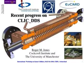
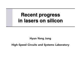
Recent progress in lasers on silicon. Hyun-Yong Jung High-Speed Circuits and Systems Laboratory. Outline. Fundamentals Silicon Raman lasers Epitaxial lasers on silicon Hybrid silicon lasers Challenges and opportunities. Fundamentals. In direct bandgap materials

E N D
Recent progress in lasers on silicon Hyun-Yong Jung High-Speed Circuits and Systems Laboratory
Outline • Fundamentals • Silicon Raman lasers • Epitaxial lasers on silicon • Hybrid silicon lasers • Challenges and opportunities
Fundamentals • In direct bandgap materials • - GaAs, InP, for example • Lowest energy points of both the • conduction & valence bands line • up vertically in the wave vector • axis • In indirect bandgap materials • - Si, Ge • Free electrons tend to reside X valley of the conduction band, which is not aligned with free holes in the valence band
Fundamentals • In indirect bandgap materials • Auger recombination • - An electron (or hole) is excited to a higher energy level by absorbing • the released energy from an electron-hole recombination • - Rate increases with injected free-carrier density & inversely • proportional to the bandgap • Free-carrier absorption (FCA) • - The free electrons in the conduction band can jump to higher energy • levels by absorbing photons • The elctrons pumped to higher energy levels release their energy through phonons
Fundamentals • Availability of nanotechnology • Breaking the crystal-symmetry or crystalline Si • A number of groups have reported enhanced light-emmiting efficiency & optical gain in low dimentional Si at low temperatures • - Porous Si, Si nanocrystals, Si-on-insulator(SOI) superlattices, Nanopillars…… • Achieving room-temperature continuous-wave lasing remains a challenge!!
Fundamentals • Advantages of Si for a good substrate • Si wafers are incredibly pure & have low defect density • 32 nm CMOS technology is sufficienty advanced to fabricate • Si has a high thermal conductivity, which is a very useful characteristic for an active device substrate • SiO2 serves as a protective layer and a naturally good optical waveguide cladding
Silicon Raman lasers • Raman Scattering (or Raman effect) • Inelastic scattering of a photon by an optical phonon • A small fraction of the scattered light(≈1/𝟏𝟎𝟕) • Raman gain coefficient in Si is around five orders of magnitude larger than that in amorphous glass fibres • Si waveguide loss is also several orders of magnitude • higher than in glass fibres • Two-photon absorption(TPA) • A nonlinear loss mechanism in which two photons combine their energies to boost an electron in the valence band to the conduction band • TPA increases with the number of photons in a waveguide • A limiting factor when using high optical pump powers
Silicon Raman lasers • Overcoming the TPA-induced FCA • A high Racetrack ring resonator Cavity • A large bend radius helps to minimize waveguide bending losses • The directional coupler is designed to utilize the pump power efficiently and achieve a low lasing threshold • TPA-induced FCA nonlinear optical loss can also reduced by optimizing the p-i-n reverse-biased diode • Silicon Raman lasers nenefit significantly from high spectral purity!!
Epitaxial lasers on silicon • Compared with Si, GaAs and InP have lattice mismatches and thermal expansion coefficient mismatches • Reducing by special surface treatment (strained superlatiices, low-temperature buffers & growth on patterned substrates) • Advanced epitaxial techniques with SiGe & GaSb buffer layers • - The realization of GaAs-based CW diode lasers on Si substrates at • room temperature • Ge-on-Si(or SiGe-on-Si) epitxial growth • - Key photonic components from this material system have demonstrated performances comparable or even better than their III-V counterparts in certain aspects
Epitaxial lasers on silicon • Germanium has an indirect band structure • ! Energy gap from the top of the valence band to the momentum-aligned Γ valley is close to the actual band gap! • The tensile strain is able to reduce the energy difference between the Γand L valleys • Strain raises the light-hole band, which increases optical gain for high injection • These techniques have enabled room-temperature direct-bandgap electroluminescence and CW room temperature optically pumped operation of Ge-on-Si lasers Optically pumped Ge-on-Si laser demonstrating CW operation at room temperature!!
Hybrid silicon lasers • It is possible to combine epitaxial films with low threading dislocation densities to the lattice-mismatched Si substrate • Advantages over bonding individual III-V lasers to a SOI host substrate The onfinement factor can be dramatically changed by changing the wave guide width
Hybrid silicon lasers • Small size, low power consumption and a short cavity design are all critical for optical interconnects • a schematic of an electrically pumped microring resonator laser, its cross-section SEM image
Hybrid silicon lasers • By lasing inside a compact microdisk III-V cavity and coupling to an external Si waveguide, a good overlap between the optical mode and electrical gain results • Schematic of a heterogeneously integrated III-V • microdisk laser with a vertically coupled SOI wave guide • Results from combining four devices with diameters • Increasing thermal impedance causes laser performance to decrease dramatically with smaller diameters A major hurdle in the realization of compact devices
Challenges and opportunities • Opportunities • Optical interconnects could be a possible solution • Achieving smaller interconnect delays, lower crosstalk & better resistance to electromagnetic interference • Integration with CMOS circuits can provide low cost, integrated control, signals processing and error correction • power consumption must be reduced to 2 pJ bit -1 or lower • Silicon Raman lasers are potentially ideal light sources for a variety of wavelength-sensitive regimes • Raman lasers will be very competitive in size and cost if a pump source can be integrated