Thermal Property Parameters
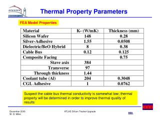
Thermal Property Parameters. FEA Model Properties. Suspect the cable bus thermal conductivity is somewhat low; thermal property will be determined in order to improve thermal quality of results. Previous Stave Geometry (Module-0W).

Thermal Property Parameters
E N D
Presentation Transcript
Thermal Property Parameters FEA Model Properties Suspect the cable bus thermal conductivity is somewhat low; thermal property will be determined in order to improve thermal quality of results ATLAS Silicon Tracker Upgrade
Previous Stave Geometry (Module-0W) Slight periodicity due to 1mm separation at beginning of each module • Stave parameters • 4.6mm semi-flattened Al tube, 12mil wall. • 192W for double sided module, 0.5W per chip, 12chips per module • Module length is 12.4cm, with row of chips nominally every 3cm • Coolant • C3F8, entering at -25ºC, assumed film coefficient of 2342W/m2K • Results • Peak chip temperature approximately -12ºC at region “A” • Module temperature nominally minus 15ºC Region “A” Note used slightly higher film coefficient than in next model ATLAS Silicon Tracker Upgrade
Revised Flat Tube Model (No Wafer Heat) Cooling tube wall -22ºC • Separation between facings 4.7mm • Modified hybrid stack, now---- • Chip, followed by silver adhesive, sitting on dielectric (5W/mK), followed by silver adhesive, sitting on BeO (240W/mK) • Before the dielectric and BeO were merged into one solid (8W/mK) • Cable K=0.4W/mK to simulate 75 micron body, whereas model thickness is 125 microns • Coolant (-25ºC, 1800W/m2K) • Film coefficient to produce about 3ºC temperature drop • Results, average chips -15.5ºC, module center area -17ºC to -17.8ºC Chips (average) Module center area ATLAS Silicon Tracker Upgrade
Revised Flat Tube Model (4W per Wafer) • Separation between facings 4.7mm • Modified hybrid stack, now---- • Chip, followed by silver adhesive, sitting on dielectric (5W/mK), followed by silver adhesive, sitting on BeO (240W/mK) • Before the dielectric and BeO were merged into one solid (8W/mK) • Cable K=0.4W/mK to simulate 75 micron body, whereas model thickness is 125 microns • Coolant (-25ºC, 1800W/m2K) • Film coefficient to produce about 3ºC temperature drop • Results, average chips -13ºC, module center area -14.5ºC to -15.3ºC Chips average Module center area ATLAS Silicon Tracker Upgrade