Download

1 / 14
140 likes | 327 Views
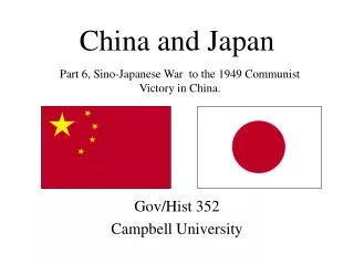
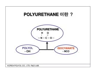
ITRS ERD/ERM in KOREA. ITRS ERD/ERM Korean Chapter Memory Committee. I. 1. oxide. 2. “ 0”. 1’. ”. V1. V0. 2’. Classification of Memory Devices. Memory Devices. Non-volatile Memory. Volatile Memory. Polarization change. Resistance change. Charge Trap. SRAM. DRAM. FLASH.

E N D
ITRS ERD/ERM Korean Chapter Memory Committee
I 1 oxide 2 “0” 1’ ” V1 V0 2’ Classification of Memory Devices Memory Devices Non-volatile Memory Volatile Memory Polarization change Resistance change Charge Trap SRAM DRAM FLASH SONOS FRAM MRAM PRAM RRAM Interface or bulk Resistance changes Phase-dependent Resistance changes Magneto- Resistance changes Charge-based Programming & Reading Current-based Programming & Reading Ref.: Samsung
ITRS ERD/ERM (Emerging Memory) Ref.: ITRS08
Next NVM Projects in Korea • Next Nonvolatile Memory Projects • 1.Period: 2005~2011, 7 years • 2. Total Budget: 50.5B K₩ (42M US$, Exchange Rate=1200K₩ ) • 3. Focus on Developing New NVM for High Density Memory NFGM PoRAM STT-MRAM ReRAM Ref.: Ministry of Knowledge and Economy 2008. 06
Strategic Approach (ex.: ReRAM) Material Develop Fundamental Study PMC Perovskite Multilayer binary oxide Binary oxide Epi-Oxide Charact. Doped binary oxide Unit cell & cell array develop (KJIST) • Materials • RS Mechanism • Memory cell • Reliability / Uniformity • Scalability (~50nm) • Cell array integration • <100nm unit process • 32 x 32 cell array • Array characterization Modeling Industry: Feedback, Tech. Support Highly Reliable ReRAM !! Ref.: Hwang
Summary of current status (ReRAM) Nanoimprint 32x32 cell array 4 inch wafer process Sub 50nm Scale device Unit cell process Mass production Ref.: Hwang
Hybrid memory in dual layer • Cu:MoOx/GdOx stack • Schematic diagram • DC I-V sweep • No switching for • Pt/Cu:MoOx/Pt • Hysteretic bipolar • switching • No Area dependence • Cycles >103 by DC Filament switching Ionic switching ∆V/σ=6.86 ∆V=2.15 ∆V/σ=5.15 • Device performance Cell Array & 4” process Ref.: Hwang
Redox / oxidation memory • Sm / LCMO stack • Motivation • DC I-V sweep • S. Muraoka et al, IEDM2007 • Unity Semiconductor, US0171200 • Device performance Analysis of Switching mechanism Ref.: Hwang
PMC memory • Cu-C memory • Motivation • Schematic diagram & DC I-V sweep • <Problem> • Low operation voltage • Retention @ high temp • <Carbon> • Porous • Small radius • Device performance Improving pulse switching Ref.: Hwang
Nanodevice using CuC (with Hynix) TE Cu-C NIT TiN W 58nm 44nm TiN Thermal oxide Si sub • Schematic diagram • DC I-V sweep Wafer provided by Hynix Split 42~66nm • Area dependence • Pulse switching • Summary Ref.: Hwang
TEM Analysis on LRS/HRS spot Pt PCMO Pt Tilt FIB Milling Oxidation OFF OFF Pt Mo Al Sm ON ON AlOx Reduction 2 2 - - 2 2 - - O O O O PCMO LCMO LRS HRS HRS • Interface sample for • TEM analysis • Evidence for the switching models HRS Pt PCMO HRS LRS Pt 30 nm 30 nm 300k Pt 10 nm PCMO 10 nm Pt HRS – Robust AlOx EDX Analysis Ref.: Hwang
Electrode Oxide Electrode Diode, ND Overview of ReRAM Operation Principle (Unipolar) - Resistance Change by Filament Formation/Rupture - On-states When Filament Formed - Off-states When Filament Rupture Cross Point Array 3D Stacking Merits - Low-cost, Simple Processes - Relatively Easy 3-D Stacking Obstacles - Unclear Mechanism - Use of Metastable Materials Strategy for Low-cost, High-density Memory Ref.: Samsung
Summary • Why ReRAM? • Scalability potential (No charge-limited) Operation at sub 20nm ?? • 4F2 Cross-point structure Requires Control Elements !! • 3-D stacking Cost effective ?? • Requirements for ReRAM • CMOS compatibility Non-noble electrode • Control elements: • Diode for unipolar switching Enough drive current ?? • Threshold switch (varistor) for bipolar switching Exist ?? • Multi-bit operation Requires large P/E window, very good distribution • Selection Rule for ReRAM ??