Download
1 / 36
370 likes | 643 Views
Photonic Band Gap Structures. Mikhail Rybin. Saint Petersburg State University, Ioffe Physico-Technical Institute. Euler School March-April 2004. Overview. Photonic crystals and photonic bandgap Artificial opals Photonic bandgap structure of artificial opals:

E N D
Photonic Band Gap Structures Mikhail Rybin Saint Petersburg State University, Ioffe Physico-Technical Institute Euler School March-April 2004
Overview • Photonic crystals and photonic bandgap • Artificial opals • Photonic bandgap structure of artificial opals: • Transmission experiments • 4. 3D diffraction of light in opals: visualization of photonic band gap structure • 5. Conclusions
Bragg Diffraction Wavelength does not correspond to the period Reflected waves are not in phase. Wave propagates through. Wavelength corresponds to the period. Reflected waves are in phase. Wave does not propagate inside.
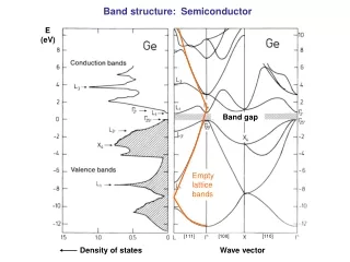
Energy gap Gap in energy spectra of electrons arises in periodic structure
Energy gap in electromagnetic spectrum Increasing of the dielectric contrast could lead to the overlapping of energy gaps in any direction in 3D space.
Width of complete band gap Calculation of bandwidth in dependence of dielectric constants S. John et al. PRE (1998)
Density of States in fcc structure There is no states in any direction within complete photonic band gap S. John et al. PRE (1998)
2D PHB Structures Sharp band waveguide channel in 2D photonic crystal Macro-porous silicon material with incorporated defect line
Artificial Phonic Structure E.Yablonovitch et al., PRL (1987, 1991) Fabrication of artificial fcc material and band gap structure for such material.
3D Photonic materials E. Yablonovitch, PRL(1989) S.Noda, Nature (1999) K. Robbie, Nature (1996) Examples of artificial photonic crystals
Artificial Opal Artificial opal sample (SEM Image) Several cleaved planes of fcc structure are shown
Artificial Opal Images of artificial opal. Left: as-growth surface (111) of the sample (SEM image) Right: surface of the (110)-oriented plane sample (AFM image)
Fabrication of artificial opals There are 3 in-layer position A – red; B – blue; C –green; Layers could pack in fcc lattice: ABCABC or ACBACB hcp lattice: ABABAB Silica spheres settle in close packed hexagonal layers
Inverted Opals Inversed opals obtain greater dielectric contrast than opals.
Diffraction on growth layers Energy of the gap in transmission and energy of the maximum in reflection spectra are coincided • Transmission for different incident angles: • 00 • 200 • 300 • 400 • 540
Band structure of diamond lattice Photonic band structure of diamond lattice (refractive index ~3.45) John et. al. PRE (1998)
Angular-resolved transmission spectra Bandgap position for different incident angle directions
Geometry of “2-spots” and “4- spots” Diffraction patterns in two different scattering geometry (Art image)
Geometry of “2-spots” and “4- spots” Diffraction patterns in two different scattering geometry (Art image)
Visualization of Photonic Band Structure in opals 1 = 515 nm 2 = 578 nm 3 = 633 nm
Conclusions • Photonic band gap structures are new class of material possessed uncial photonic properties. Opal-based structures are 3D photonic crystals. • 2. Photonic band gap structure was obtained for artificial opals in the visible range from angle-resolved transmission measurements. • 3. Photonic band gap structure could be visualized by diffraction method. Diffraction patterns provides information about structure of photonic crystal.
Spontaneous Emission Control Emission is forbidden if energy of photonic bandgap and width of electron’s energy gap are coincided.