Download
1 / 8
90 likes | 553 Views
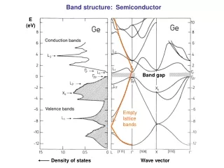
This comprehensive overview explores the band structure of semiconductors and transition metals, focusing on concepts such as the band gap, density of states, and wave vectors. It discusses the differences between empty lattice bands, experimental measurements, and theoretical models. Key attention is given to the unique properties of graphite's π-bands and topological insulators, highlighting their distinct energy dispersion and metallic surface states. This text serves as a guide to understanding the behavior of electrons in various materials, from noble metals like copper to semiconductors like germanium.

E N D
E (eV) Band gap Empty lattice bands Density of states Wave vector Band structure: Semiconductor [111] [100] [110]
Inverse photoemission Photoemission “Empty lattice solution” vs. Experimental bands E(k) = ħ2/2me (k+Ghkl)2 + V0 Experiment + full theory (lines) E (2eV) E (5eV) Ge (200) (111) Vacuum level EV EV =0 (-111) CBM VBM (-200) (1-1-1) Ghkl = (-1-1-1) (2/a) (000) V0 V0 k L =(000) k L=(½½½)
1 2 d-bands 4 3 1 1 s,p-band (like a free electron) d-bands (like atomic energy levels) Band structure: Noble metal Cu [111] [110]
Ni Fermi level s,p-band (like a free electron) d-bands (like atomic energy levels) Band structure: Transition metal Ni Cu Rigid band model (one less e in Ni)
Delocalized s-electrons vs. localized d-electrons Wave functions of the outer electrons versus distance (in Å = 0.1 nm) for nickel, a transition metal. The 4s electrons are truly metallic, extending well beyond the nearest neighbor atoms (at r1, r2, r3 ). The 3d electrons are concentrated at the centralatomandbehavealmostlikeatomicstates.TheycarrythemagnetisminNi. (r) r (Å)
Two-dimensional -bands of graphene E[eV] Empty EFermi Occupied K =0 M K Empty * kx,y M K Occupied In two dimensions one has the quantum numbers E,kx,y. This plot of the energy bands shows E vertically and kx ,ky in the horizontal plane.
“Dirac cones” in graphene A special feature of the graphene -bands is their linear E(k)dispersion near the six corners K of the Brillouin zone (instead of the parabolicrelationfor free electron bands). In a plot of E versus kx,ky one obtains cone-shaped energy bands attheFermi level.
Topological Insulators A spin-polarized version of a “Dirac cone” occurs in “topological insulators”. These are insulators in the bulk and metals at the surface, because two surface bands bridge the bulk band gap. It is impossible topologically to remove the surface bands from the gap, because they are tied to the valence band on one side and to the conduction band on the other. The metallic surface state bands have been measured by angle- and spin-resolved photoemission.