Advances in Flexible OLED Technologies and Substrate Innovations
This document explores the cutting-edge developments in flexible OLED (Organic Light Emitting Diodes) technologies, particularly focusing on substrate materials. OLEDs stand out by eliminating the need for a backlight and achieving unprecedented thinness, with the potential for 2 mm thick screens, surpassing traditional LCDs. Key areas of discussion include polymer and flexible glass substrates, their processing challenges, and stress management techniques to ensure durability. Supported by US Army funding, this research aims to revolutionize display technologies with high-performance materials.

Advances in Flexible OLED Technologies and Substrate Innovations
E N D
Presentation Transcript
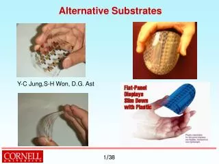
Alternative Substrates Y-C Jung,S-H Won, D.G. Ast
The biggest strength of OLEDs is that they do not require a backlight and can be made thinnerthan any other technology used today. A 2 mm thick OLED is a reality today where the thinnest LCD is 3 mm” Sharp http://www.sharpsma.com/lcd/lcdguide/Technologies/Tech_index.php
The US Army provided the core funding of $43.7 M to establish the Flexible Display Center at ASU. www.asu.edu/ia/photogallery/fdc/1.htm
Outline 1 Overview 2 Polymer Substrates 3. Flexible Glass Substrates 4. Processing Corning Microsheet 5. Results 6. Summary
Polymers Borosilicate Glass 1. Overview T< 600 °C T < 300 °C CTE PET 65 • 10-6/oC) CTE 00 MS 7.4 • 10-6/oC) CTE Si 2.6 •10-6/oC) CTE Si 2.6 •10-6/oC) -Si:H α-Si:H ELA poly-Si + 1m SiO2 LPCVD poly-Si LTO MILC silicon ELA poly-Si LTO, Annealed LTO Better match: Glass !
2. Polymer Substrates Uncoated : Oxygen, Water Transmission: 1… 100 g/m2/ day Coated with 4 inorganic layer (Vitex)
Elaborate Adhesion and Stress Management required Up to 13 inorganic layers with CTE 1/30’th of polymer may have to be deposited on polymer! “Due to accumulated internal stresses, optimisation of composition, stress and adhesion for each layer is needed in order to avoid warping of the substrate and cracking of the layers during deposition and/or laser annealing. Such stresses arise, for the most part, from difference in CTE of the plastic substrate and inorganic layers”. SID 03 Digest. Paper 47.1 High Performance Plastic Substrates for Active Matrix Flexible FPD. Simone Angiolini, Mauro Avidano, Roberto Bracco, Carlo Barlocco Specialty Materials, Ferrania Imaging Technologies, Italy ; Nigel D. Young, Michael Trainor Philips Research Laboratories, UK; Xiao-Mei Zhao Electronic Materials, Promerus LLC, USA]
The most difficult step of poly-Si on plastics Electronics PECVD SiO2 must be 5 to 10 times thicker than channel www.FlexIcs.com
Plastics on semiconductor technology is not new ..but difficult to manufacture and commercialize Intel-funded plastic IC firm folds, assets up for sale
3. Flexible Glass Substrates • Solve most of CTE induced stress problems • Permit process temperatures in excess of 600 oC • Can use sintered semiconductors (e.g. inkjet printed nano-slurries) • Are available from two rivaling glass companies
Corning 0211 Microsheet Borosilicate Glass ~50…~100m (00,0) CTE : 7.4….8.4 x 10-7/oC
Commercial Products Corning MicrosheetSchott D263 SiO2 (65wt%) SiO2 (64%), Al2O3 (2wt%)……dopant Al2O3(4%), B2O3 (9wt%)…….. Dopant B2O3(8%), Na2O (7wt%)……. GB r collapseNa2O 6%, K2O (7wt%) …….. GB r collapse ZnO (7wt%) ……. Deep state: 0.3,0.6eV 3% not listed 18% not listed
Mechanical Properties(Schott D 263) Influence of edge and surface coating on strength. R=30mm; pfail <1% Fracture strength of glass A upper edge (initial scribing) and B lower edge. Radii of 30 mm; failure < 1% Armin Plichta, Andreas Habeck, Silke Knoche, Anke Kruse, Andreas Weber, Norbert Hildebrand in Ch. 3 “Flexible Glass Substrates” in “Flexible Flat Panel Displays”, Wiley-SID Series in DisplayTechnology, Ed.: Gregory P. Crawford, ISBN: 9780470870488 Online ISBN: 9780470870501;
4 Processing Microsheet 4.1 Options to process flexible, ultra-thin glass in a conventional line 1. Anodic Bonding to a Si wafer, release via release a la surface MEMS 2. Peripheral Anodic Bonding to Si wafer, release by cutting, sacrificing edge 3. Anodic bonding to flexible Si structures, e.g. pillars, springs 4. Floating on liquid metal 5. Minature version of susceptor slot, created on carrier wafer
Anodic Bonding, 350oC, 10N, 1000V Failure mode: Delayed fracture, driven by 0.2% residual tensile strain
GaxIn1-x bonding Failure mode: Microsheet edge lift of during CNF required RCA clean
“Pocket” carrier system, fabricated on 4” Si wafer: Rectangular substrate, diamond cut, good edge finish
4 Processing Microsheet 4.2 Processes Used to fabricate TFTs on oxidized Si and Microsheet 4.2.1 Furnace Mixed (580oC) precursor + 600…620oC Furnace Anneal (Oxidized 4” Si) 4.2.2 RTA Mixed (580oC) precursor + 650oC Rapid Thermal Annealin 4.2.3 ELA Amorphous (500oC) precursor + Excimer Laser Annealing
Poly-Si TFT Structure Baseline on oxidized Si wafer Barrier coated Microsheet
4. Results 4.1. Mixed amorphous/x-stalline 580oC precursor 620oC, 24 hr Anneal
Mixed a/x-stalline Si Precursor: Structure <111> peak of Poly Si TEM XRD <220> <311> Mixed Si 150 nm deposited at 580oC LPCVD (silane) Temp : 580 oC Time : 30 min
TEM of mixed amorphous, crystalline precursor, To be converted (620oC furnace, 650oC RTA) to fully poly-Si film.
Transfer Characteristics Vd(V) 10 5 0.1 Vg(V) 40 30 20 10 * a/x-stal mixture active layer: 580°C, 100nm * Gate oxide (LTO): 400°C, 100nm * W/L = 55um/8um * Channel Mobility 7 cm2/Vs
Hydrogenation - H2 PECD System 300 oC, 80 sccm, 600 mTorr, 350W 580oC precursor; 620oC, 24 hrs, Reference wafer
B.L. deposition BL at 620oC Anneal Failure Mode: Shorts CTE increases > 5500C Cool down - Cracks close - undetectable Doremus: Glass Science. Jon Wiley and Sons
Boron Profile after 24hr , 620oC Anneal poly SiO2 SiNx Microsheet
Failure Mode Summary • Devices failed as shorts (100%) • Traced to non-linear CTE of MS glass approaching Tg • Failure by CTE mismatch to barrier layer - not device silicon • A more SiO2 rich substrate (not commercially available) would . solve problem
4. Results (continued) Mixed amorphous/x-stalline 580oC precursor 650oC, 100 Pulse RTA Anneal
TFT on Microsheet - 650°C, 100 Pulse - Pulse time: 5 sec Low yield * a/x-stal precursor: 580°C, 100nm * Gate oxide (LTO): 400°C, 100nm
4. Results (continued) Excimer Laser Processing
XRD of ELA annealed 500oC a-Si) 124~361 mJ/cm2, single pulse
ELA; 500oC a-Si ; 274 mJ/cm2 ; Oxidized Si Vg(V) 40 30 20 10 Vd(V) 10 5 *a-Si active layer: 500°C, 100nm * Gate oxide (LTO): 400°C, 100nm * Annealing (500 °C, 4hrs.)
ELA ; 500oC a-Si ; 274 mJ/cm2 ELA; Microsheet Vd(V) 10 5 Vg(V) 45 35 25 *a-Si active layer: 500°C, 100nm * Gate oxide (LTO): 400°C, 100nm * Annealing (500 °C, 4hrs.)
Failure Mode Open - indicating insufficient doping activation Channel Resistivity ~ 106Wcm indicative of undoped poly-Si
Summary 1. Three methods to process Microsheet carry Microsheet in a line explored: a) Anodic bonding (full and partial) to 4” wafer b) InGa bonding to 4” wafer c) a MEMS fabricated carrier on 4” Si. 2. Three TFT processes investigated on two substrates (Microsheet, Si): - Amorphous Si with x-stal nuclei + 600 to 620 °C Furnace anneal - Amorphous Si with x-stal nuclei + 650 RTA anneal, Gla - Amorphous Si + Excimer Laser Annealing (ELA) 3. The upper temperature at which TFTs can be fabricated by cw (furnace) or (RTA) anneal limited by CTE difference between MS and the SiO2/SiNx barrier layer. Above about 550 °C, barrier layer fails in tension, permitting the out-diffusion of Boron which in turn shortens the TFT source to drain.
Summary (continued) 4. Poly-Si TFTs can be fabricated on Microsheet with ELA (Excimer Laser Annealing using power densities of about 280 mJ/cm2) 5. Future work ELA fabricated TFTs with hydrogen passivation from PECVD Nitride and simultaneous LTO densification using dummy absorber Acknowledgements This investigation was carried out with the financial support of Corning Inc. at the Cornell Nanofabrication Center, an NSF supported node in NSF NNUN network.