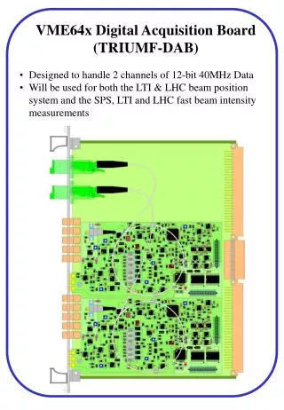
Digital Board
Digital Board. How to write a Simple Xilinx Program. First launch the Xilinx software program Xilinx ISE 11 When the program opens, select New Project or File -> New Project The following window will start. Digital Board.


Digital Board
E N D
Presentation Transcript
Digital Board How to write a Simple Xilinx Program • First launch the Xilinx software program • Xilinx ISE 11 • When the program opens, select • New Project • or File -> New Project • The following window will start
Digital Board • Put in a project name, select a project location (may browse to select location [thumb drive]; best with no spaces in name) • Make sure to select schematic • Select Next
Digital Board • Enter in all data as shown on right • Select Next
Digital Board • Create a new source file by clicking New Source • Highlight “Schematic” and enter in a file name • Select Next, then Finish, (then Yes if needed to create directory), then Next, Next, and Finish; then be patient …
Digital Board • This is what the screen looks like • Click on Lab4.sch to see the blank schematic
Digital Board • Type in OR2 in the ‘Symbol Name Filter’ box then click and highlight the ‘or2’ in the ‘Symbols (that begin with …)’ box. • Move the mouse onto the schematic and you will see the 2 input OR gate. • Put a 2input OR gate, a 2 input AND (and2) gate and an inverter (inv) on the schematic as shown next
Digital Board • Use the wiring tool to connect the symbols (you may have to zoom in, ctrl+mousewheel)
Digital Board • Use the IO Marker tool to connect inputs and outputs • You may need to specify “Add an input marker” (or output) in the “Properties” window [accessed by the ‘Options’ menu]
Digital Board Select tool to select an item • Use select tool • Rename IO markers. Inputs are A, B, C and output is X. Double click on the IO markers or the net. Rename the ‘Nets’ item • Click on Design to finish the design
S3E Board Switches and Lights • The pins assigned in the next step correspond to switches on the board (inputs) and an LED (output).
Digital Board • Right Click on “Lab4” and Select “Add Copy of Source” • In “File Name” box type: \\AUS206L22\CompE224_filesand hit return, then select “lab4.ucf” • Select “Open” • Select “Ok” in the “Adding Source Files …” dialog box • Save all changes (icon or under ‘File’) Save all changes
UCF File • Click the “+” next to Lab4, and select the “Lab4.ucf” file • Click the “+” in the Process window next to “User Constraints”, Double click on “Edit Constraints (Text)” to view .ucf file • Select “Lab4” to return to the main “Processes” sub-window • Click on lab4.sch to see schematic
To Create The UCF File Manually (1 of 4) • Select • New Source …
To Create The UCF File Manually (2 of 4) • Select • Next > • Finish
To Create The UCF File Manually (4 of 4) • Type NET lines as shown. • Select File | Save
Digital Board • Select lab4 • Double click “Implement Design” in Processes window • When done, it should look like(might be orange) • You are now ready to download and test
Digital Board • Double click “Generate Programming File” in the Processes window (you should get a check mark) • If you get a dialog box • Click Decline • Choose “Disable the collection of device usage statistics for all projects” • Click OK • Click OK
Xilinx BoardConnections • Connect your Xilinx board to the PC with the USB cable (wear the wrist band) • Use the USB ports on the front of the PC • Make sure to not try to plug in the other end of the USB cable into the Ethernet port that is next to the USB port on the Xilinx board • Plug your board into the power supply • There is no hole cut in the plastic cover to be able to access the on/off switch on the board. Plug / unplug the power connector to turn the board on and off.
Double click Configure Target Device Click Okay Opens ISE iMPACT Digital Board
Digital Board • Double click Boundary Scan • Right click in ISE iMPACT main window and select “Initialize Chain” • Click yes
Digital Board • Go to the current lab directory • Click lab4.bit and then Open • Click No then Bypass two times • Click Ok[Device 1 (FPGA xc3s5003) should be highlighted]
Digital Board • Right click the first chip diagram and select “Program” • The FPGA will be programmed • Test the design using the switches • Save your design