Download
1 / 18
190 likes | 515 Views
Silicon Carbide X-Ray detectors for Planetary Exploration. Dr. John E. Lees University of Leicester 8 th International Conference on Position Sensitive Detectors September 2008. Introduction. Limitations of silicon based detectors for planetary exploration cooling radiation damage

E N D
Silicon Carbide X-Ray detectors for Planetary Exploration Dr. John E. Lees University of Leicester 8th International Conference on Position Sensitive Detectors September 2008
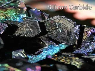
Introduction • Limitations of silicon based detectors for planetary explorationcoolingradiation damage • Search for other materials – wide band gapGaAs • DiamondSilicon Carbide • SiC imaging arrays Collaboration with University of Newcastle
SiC X Ideal requirements for X-ray detectors • Photon counting • Imaging • Good timing resolution • High spatial resolution • Solar blind – not sensitive to visible light • High quantum efficiency • High dynamic range • Low background • Radiation hard • Energy resolution
1.81x10⁻³cm-2 1.0x10⁻³cm-2 4.93x10⁻⁴cm-2 400m Semi-Transparent SiC Schottky Diode • LHS: A 280m2 Schottky contact and gold bond pad • RHS: Die layout with a range of diode sizes
Semi-transparent Schottky contact. 3 nm Ti / 12 nm Ni 25 nm thermallygrown SiO2 4nm Cr / 200nm Au n 4H-SiC n+ 4H-SiC 5 nm Cr / 250nm Au • 4nmCr/100nmNiOhmic Contact STSSD structure • 20 m epitaxial layer on a 370 m substrate Lees et al.,Nucl. Inst. Meth A 578 (2007) 266-234
Improving the Low Energy Response • K-shell emission lines of elements: Na (Z=11, E=1.04 keV) to Zn (Z=30, E=8.64 keV) STSSD has an 18nm thick electrode
Planetary Exploration • General Multi-spectral: X-rays/UV/Optical/Infra-red • Imaging pixel arrays • Environment Radiation environment • Shielding • Radiation hard electronics • Operating temperatures • Spacecraft Mass • Power • Cost
Some current and planned planetary missions • Mercury Messenger and BepiColombo • Venus Venus Express and Venus Climate Orbiter • Mars Mars Reconnaissance Orbiter, Mars Express, ExoMars • Saturn Cassini-Huygens and Tandem • Jupiter JUNO and Laplace
Jupiter FUV (HST) X-rays (Chandra)
Auroral Processes • Precipitation of energetic ions and electrons along field lines from the planetary magnetosphere into the atmosphere produces emissions in IR, visible, UV, and X-ray wavelengths • Table shows typical values for the magnetised planets • Planet Earth Jupiter Saturn Uranus Neptune • Electron input power (GW)10 1000 100 10 1 • UV output (GW)1 100 10 1 0.1 • X-ray brem output (MW)1 100 10 1 0.1
Radiation environment Alessandro Atzei and Peter Falkner, ESA technical note, SCI-AP/2004/TN-085/AA
Radiation environment Comparison between ONERA-full (D&G + GIRE + Salammbô) and ESA ref. D&G at an equatorial distance of 3 Rj from Jupiter centre
Irradiation of STSSDs • Phase 1 - irradiation at Paul Scherrer Institut • 63 MeV protons • Total fluence 1x1011 cm-2 • Phase 2 - irradiation at Theodor Svedberg Laboratory • 50 MeV. • Total fluence ~1 x 10¹³ protons cm-2.
STSSD Radiation Tolerance • I-V measurements
STSSD Radiation Tolerance • 55Fe X-ray spectra
STSSD Radiation Tolerance • 109Cd X-ray spectra
Next Steps • Material characterisation • Improve electronics better energy resolution • Extend radiation fluences • Protons, neutrons, electrons and X-ray/gamma-ray • Modelling • New device structures
Acknowledgements • Nigel Bannister University of Leicester • David Bassford • Emma Bunce • Stan Cowley • George Fraser • Mark Sims • Dean Talboys • Chris Whitford • Alton Horsfall University of Newcastle