Download
1 / 8
80 likes | 215 Views
This document outlines key learning opportunities from ASIC1 to inform ASIC2 developments, focusing on logic test structures. It presents a comprehensive checklist for testing, including labelling accuracy, threshold scans, spatial data analysis, and efficiency evaluations of sensor performance. Critical bug fixes and suggested modifications for PCB designs, along with potential sensor advancements, are discussed. Future directions include detailed explorations into noise performance and power management, while emphasizing the necessity for robust testing mechanisms for seamless integration into larger pixel arrays.

E N D
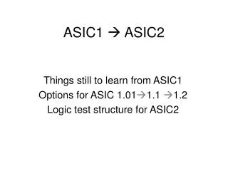
ASIC1 ASIC2 Things still to learn from ASIC1 Options for ASIC 1.011.1 1.2 Logic test structure for ASIC2
Things still to learn from ASIC1 Test beam • Check labelling & operating conditions of hits-per-BT plot (back/red) • Threshold scans of all sensors shown together, one plot for each of the four pixel architectures • Spatial info – locations of noisy pixels • Statistics of hits – beam profile? • Per-pixel efficiency? Laser • Bias optimisation for signal/noise • Automated scan of every pixel to compare gain/noise • Crosstalk analysis –scan around a 9x9 block of pixels – vs threshold • Linearity Bench • Threshold scan with VTH signals buffered / externally driven • Full speed operation (189ns bunch crossing rate) • Noise vs temperature
Possible next sensors Sensor 1.01(4 seats silicon)PCB 1.0 • bug fix SRAM write with full 3.3v level-shifting • bug fix monostables (IOUTBIAS mirror transistors) • bug fix ISENSEBIAS mirror transistor • add nwell diodes around test structure pixels • larger bond pads? Sensor 1.1(4 seats silicon) PCB 1.1 • add preShape test structures 2nd hole for laser • extra pads? Sensor 1.2(4 seats silicon) PCB 1.X • add analog buffers for VTH and VRST signals? • reduce / change pixel variants? • tweak pixel design for noise/gain performance? • … 4 weeks 3 weeks 24/3 ~ 8 weeks 19/5
Possible next sensors Logic/Support Test Structure(+1 seat silicon) New test PCB(s) required • Large pad-over-logic pad cells for bump-bond tests • LVDS receiver and transmitter pad circuits • Gray code counter for timestamp generation • Clock generator (makes all sensor internal clocks from one external clock) • Bunch train state machine • Readout state machine • Master controller (co-ordinates preceding logic blocks, resets, power-on safe states) • Configuration controller (co-ordinates mask & trim programming, adding on-chip registers for current/voltage DACs etc. • Current DAC circuits • Voltage DAC circuits • … 14/7 12 weeks 15/9
ASIC2 Sequencer Overview Small test pad? OVRD OVERRIDE HOLD MUX[2:0] TIMECODE[12:0] INIT FWD PHI1 PHI2 PHI3 LATCHSAFE OF[7:0] MSOPOR PIXEL RESETS PIXEL ENABLE SENSE_ENABLE READENABLE[7:0] ORE[7:0] MUX[2:0] DATA[30:0] Bunch train state machine MODE0 MODE1 • MODE SEL • PRE-SPILL • SPILL • READ • IDLE En Clk Gen Master REFCLK Readout state machine En TOKIN TOKOUT SDATA
ASIC2 Services BIAS1 BIAS2 BIAS3 BIAS4 VTH+ VTH- Vcasc1 Vcasc2 Current biases Sensor ID code …to readout unit Setup registers DOUT Voltage DACs DOUT_RDBK PHI1 PHI2 FAST PHI3 PHI1 PHI2 SLOW PHI3 PHI1 PHI2 RDBK PHI3 DIN_CONFIG Config controller CLK DIN
Example “1-seat” logic test structure • 240um bump bondable pads on 1mm pitch • Small wire-bond pads to test the generated logic signals 500x750 um logic blocks Wire bond pads for testing Bump bond pads • Implement as many of the logic blocks and signal distribution as possible • Folded design models a full-width logic slice serving a large array of pixels
ASIC2 Concept • Logic columns • Power pads over the logic used to distribute global power supplies • Central row of control logic • 500um profile • Bump Bond Pads for control & IO signals • Clocks • Synchronisation • Mode • Configuration • Serial data out • Power