- Enhancing Performance with Configurable Computing -
Configurable computing allows for real-time customization of hardware function, improving performance in signal processing, encryption, and more. Learn how this adaptability benefits various applications. -

- Enhancing Performance with Configurable Computing -
E N D
Presentation Transcript
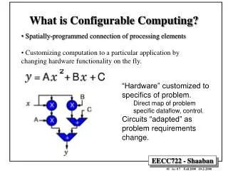
What is Configurable Computing? • Spatially-programmed connection of processing elements • Customizing computation to a particular application by changing hardware functionality on the fly. • “Hardware” customized to specifics of problem. • Direct map of problem specific dataflow, control. • Circuits “adapted” as problem requirements change.
Spatial vs. Temporal Computing Temporal Spatial
Why Configurable Computing? • To improve performance over a software implementation • e.g. signal processing apps in configurable hardware • To improve product flexibility compared to hardware • e.g. encryption or network protocols in configurable hardware • To use the same hardware for different purposes at different points in the computation.
Configurable Computing Application Areas • Signal processing • Encryption • Low-power (through hardware "sharing") • Variable precision arithmetic • Logic-intensive applications • In-the-field hardware enhancements • Adaptive (learning) hardware elements
Sample Configurable Computing Application:Prototype Video Communications System • Uses a single FPGA to perform four functions that typically require separate chips. • A memory chip stores the four circuit configurations and loads them sequentially into the FPGA. • Initially, the FPGA's circuits are configured to acquire digitized video data. • The chip is then rapidly reconfigured to transform the video information into a compressed form and reconfigured again to prepare it for transmission. • Finally, the FPGA circuits are reconfigured to modulate and transmit the video information. • At the receiver, the four configurations are applied in reverse order to demodulate the data, uncompress the image and then send it to a digital-to-analog converter so it can be displayed on a television screen.
Early Configurable Computing Successes • Fastest RSA implementation is on a reconfigurable machine (DEC PAM) • Splash2 (SRC) performs DNA Sequence matching 300x Cray2 speed, and 200x a 16K CM2 • Many modern processors and ASICs are verified using FPGA emulation systems • For many signal processing/filtering operations, single chip FPGAs outperform DSPs by 10-100x.
Computes one function (e.g. FP-multiply, divider, DCT) Function defined at fabrication time Parameterizable Hardware: Performs limited “set” of functions Defining Terms Fixed Function: Programmable: • Computes “any” computable function (e.g. Processor, DSPs, FPGAs) • Function defined after fabrication
Conventional Programmable ProcessorsVs. Configurable devices Conventional Programmable Processors • Moderately wide datapath which have been growing larger over time (e.g. 16, 32, 64, 128 bits), • Support for large on-chip instruction caches which have been also been growing larger over time and can now hold hundreds to thousands of instructions • High bandwidth instruction distribution so that several instructions may be issued per cycle at the cost of dedicating considerable die area for instruction distribution • A single thread of computation control. Configurable devices (such as FPGAs): • Narrow datapath (e.g. almost always one bit), • On-chip space for only one instruction per compute element -- i.e. the single instruction which tells the FPGA array cell what function to perform and how to route its inputs and outputs • Minimal die area dedicated to instruction distribution such that it takes hundreds of thousands of compute cycles to change the active set of array instructions
Field programmable gate arrays (FPGAs) • Chip contains many small building blocks that can be configured to implement different functions. • These building blocks are known as CLBs (Configurable Logic Blocks) • FPGAs typically "programmed" by having them read in a stream of configuration information from off-chip • Typically in-circuit programmable (As opposed to EPLDs which are typically programmed by removing them from the circuit and using a PROM programmer) • 25% of an FPGA's gates are application-usable • The rest control the configurability, etc. • As much as 10X clock rate degradation compared to custom hardware implementation • Typically built using SRAM fabrication technology • Since FPGAs "act" like SRAM or logic, they lose their program when they lose power. • Configuration bits need to be reloaded on power-up. • Usually reloaded from a PROM, or downloaded from memory via an I/O bus.
Programmable Circuitry • Programmable circuits in a field-programmable gate array (FPGA) can be created or removed by sending signals to gates in the logic elements. • A built-in grid of circuits arranged in columns and rows allows the designer to connect a logic element to other logic elements or to an external memory or microprocessor. • The logic elements are grouped in blocks that perform basic binary operations such as AND, OR and NOT • Several firms, including Xilinx and Altera, have developed devices with the capability of 100,000 equivalent gates.
Look-Up Table (LUT) In Out 00 0 01 1 10 1 11 0 Mem Out 2-LUT In2 In1
LUTs • K-LUT -- K input lookup table • Any function of K inputs by programming table
Conventional FPGA Tile K-LUT (typical k=4) w/ optional output Flip-Flop
XC4000 CLB Cascaded 4 LUTs (2 4-LUTs -> 1 3-LUT)
Programming/Configuring FPGAs • Software (e.g. XACT or other tools) converts a design to netlist format. • XACT: • Partitions the design into logic blocks • Then finds a good placement for each block and routing between them (PPR) • Then a serial bitstream is generated and fed down to the FPGAs themselves • The configuration bits are loaded into a "long shift register" on the FPGA. • The output lines from this shift register are control wires that control the behavior of all the CLBs on the chip.
Configurable Computing Architectures • Configurable Computing architectures combine elements of general-purpose computing and application-specific integrated circuits (ASICs). • The general-purpose processor operates with fixed circuits that perform multiple tasks under the control of software. • An ASIC contains circuits specialized to a particular task and thus needs little or no software to instruct it. • The configurable computer can execute software commands that alter its FPGA circuits as needed to perform a variety of jobs.
Hybrid-Architecture Computer • Combines a general-purpose microprocessor and reconfigurable FPGA chips. • A controller FPGA loads circuit configurations stored in the memory onto the processor FPGA in response to the requests of the operating program. • If the memory does not contain a requested circuit, the processor FPGA sends a request to the PC host, which then loads the configuration for the desired circuit. • Common Hybrid Configurable Architecture Today: • FPGA array on board connected to I/O bus • Future Hybrid Configurable Architecture: • Integrate a region of configurable hardware (FPGA or something else?) onto processor chip itself • Integrate configurable hardware onto DRAM chip=> Flexible computing without memory bottleneck
Benefits of Re-Configurable Logic Devices • Non-permanent customization and application development after fabrication • “Late Binding” • economies of scale (amortize large, fixed design costs) • time-to-market (evolving requirements and standards, new ideas) Disadvantages • Efficiency penalty (area, performance, power) • Correctness Verification
Spatial/Configurable Benefits • 10x raw density advantage over processors • Potential for fine-grained (bit-level) control --- can offer another order of magnitude benefit • Locality. Spatial/Configurable Drawbacks • Each compute/interconnect resource dedicated to single function • Must dedicate resources for every computational subtask • Infrequently needed portions of a computation sit idle --> inefficient use of resources
Technology Trends Driving Configurable Computing • Increasing gap between "peak" performance of general-purpose processors and "average actually achieved" performance. • Most programmers don't write code that gets anywhere near the peak performance of current superscalar CPUs • Improvements in FPGA hardware: capacity and speed: • FPGAs use standard SRAM processes and "ride the commodity technology" curve • Volume pricing even though customized solution • Improvements in synthesis and FPGA mapping/routing software • Increasing number of transistors on a (processor) chip: How to use them all? • Bigger caches. • SMT • IRAM • Multiple processors. • FPGA!
Overall Configurable Hardware Approach • Select portions of an application where hardware customizations will offer an advantage • Map those application phases to FPGA hardware • hand-design • VHDL => synthesis • If it doesn't fit in FPGA, re-select application phase (smaller) and try again. • Perform timing analysis to determine rate at which configurable design can be clocked. • Write interface software for communication between main processor and configurable hardware • Determine where input / output data communicated between software and configurable hardware will be stored • Write code to manage its transfer (like a procedure call interface in standard software) • Write code to invoke configurable hardware (e.g. memory-mapped I/O) • Compile software (including interface code) • Send configuration bits to the configurable hardware • Run program.
Configurable Hardware Application Challenges • This process turns applications programmers into part-time hardware designers. • Performance analysis problems => what should we put in hardware? • Choice and granularity of computational elements. • Choice and granularity of interconnect network. • Hardware-Software Co-design problem • Synthesis problems • Testing/reliability problems.
The Choice of the Computational Elements Reconfigurable Logic Reconfigurable Datapaths Reconfigurable Arithmetic Reconfigurable Control Bit-Level Operations e.g. encoding Dedicated data paths e.g. Filters, AGU Arithmetic kernels e.g. Convolution RTOS Process management
Reconfigurable Processor Tools Flow Customer Application / IP (C code) RTL HDL C Compiler Synthesis & Layout ARC Object Code Configuration Bits Linker Chameleon Executable Development Board C Model Simulator C Debugger
Hardware Challenges in using FPGAs for Configurable Computing • Configuration overhead • I/O bandwidth • Speed, power, cost, density • High-level language support • Performance, Space estimators • Design verification • Partitioning and mapping across several FPGAs
PRISM (Brown) PRISC (Harvard) DPGA-coupled uP (MIT) GARP, Pleiades, … (UCB) OneChip (Toronto) REMARC (Stanford) Configurable Hardware Research • NAPA (NSC) • E5 etc. (Triscend)
Hybrid-Architecture RC Compute Models • Unaffected by array logic: Interfacing • Dedicated IO Processor. • Instruction Augmentation: • Special Instructions / Coprocessor Ops • VLIW/microcoded extension to processor • Configurable Vector unit • Autonomous co/stream processor
Logic used in place of ASIC environment customization external FPGA/PLD devices Example bus protocols peripherals sensors, actuators Hybrid-Architecture RC Compute Models:Interfacing • Case for: • Always have some system adaptation to do • Modern chips have capacity to hold processor + glue logic • reduce part count • Glue logic vary • valued added must now be accommodated on chip (formerly board level)
Triscend E5 Example: Interface/Peripherals
Array dedicated to servicing IO channel sensor, lan, wan, peripheral Provides protocol handling stream computation compression, encrypt Looks like IO peripheral to processor Hybrid-Architecture RC Compute Models:IO Processor • Maybe processor can map in • as needed • physical space permitting • Case for: • many protocols, services • only need few at a time • dedicate attention, offload processor
TBT ToggleBusTM Transceiver System Port CR32 CompactRISCTM 32 Bit Processor RPC Reconfigurable Pipeline Cntr ALP Adaptive Logic Processor CIO Configurable I/O PMA Pipeline Memory Array BIU Bus Interface Unit External Memory Interface SMA Scratchpad Memory Array CR32 Peripheral Devices NAPA 1000 Block Diagram
NAPA 1000 as IO Processor SYSTEM HOST Application Specific Sensors, Actuators, or other circuits System Port NAPA1000 CIO Memory Interface ROM & DRAM
Hybrid-Architecture RC Compute Models:Instruction Augmentation • Observation: Instruction Bandwidth • Processor can only describe a small number of basic computations in a cycle • I bits 2I operations • This is a small fraction of the operations one could do even in terms of www Ops • w22(2w) operations • Processor could have to issue w2(2 (2w) -I) operations just to describe some computations • An a priori selected base set of functions could be very bad for some applications
Instruction Augmentation • Idea: • provide a way to augment the processor’s instruction set • with operations needed by a particular application • close semantic gap / avoid mismatch • What’s required: • some way to fit augmented instructions into stream • execution engine for augmented instructions • if programmable, has own instructions • interconnect to augmented instructions
First Efforts In Instruction Augmentation • PRISM • Processor Reconfiguration through Instruction Set Metamorphosis • PRISM-I • 68010 (10MHz) + XC3090 • can reconfigure FPGA in one second! • 50-75 clocks for operations
PRISM (Brown) • FPGA on bus • access as memory mapped peripheral • explicit context management • some software discipline for use • …not much of an “architecture” presented to user
PRISM-1 Results Raw kernel speedups
PRISC (Harvard) • Takes next step • what look like if we put it on chip? • how integrate into processor ISA? • Architecture: • couple into register file as “superscalar” functional unit • flow-through array (no state)
PRISC ISA Integration • Add expfu instruction • 11 bit address space for user defined expfu instructions • fault on pfu instruction mismatch • trap code to service instruction miss • all operations occur in clock cycle • easily works with processor context switch • no state + fault on mismatch pfu instr
All compiled working from MIPS binary <200 4LUTs ? 64x3 200MHz MIPS base PRISC Results
Chimaera (Northwestern) • Start from PRISC idea • integrate as functional unit • no state • RFUOPs (like expfu) • stall processor on instruction miss, reload • Add • manage multiple instructions loaded • more than 2 inputs possible
“Live” copy of register file values feed into array Each row of array may compute from register values or intermediates (other rows) Tag on array to indicate RFUOP Chimaera Architecture
Chimaera Architecture • Array can compute on values as soon as placed in register file • Logic is combinational • When RFUOP matches • stall until result ready • critical path • only from late inputs • drive result from matching row
GARP (Berkeley) • Integrate as coprocessor • similar bwidth to processor as FU • own access to memory • Support multi-cycle operation • allow state • cycle counter to track operation • Fast operation selection • cache for configurations • dense encodings, wide path to memory
GARP • ISA -- coprocessor operations • issue gaconfig to make a particular configuration resident (may be active or cached) • explicitly move data to/from array • 2 writes, 1 read (like FU, but not 2W+1R) • processor suspend during coproc operation • cycle count tracks operation • array may directly access memory • processor and array share memory space • cache/mmu keeps consistent between • can exploit streaming data operations
Row oriented logic denser for datapath operations Dedicated path for processor/memory data Processor not have to be involved in arraymemory path GARP Array