Download
1 / 42
420 likes | 611 Views
Ch 10. Case Studies in Sequential Logic Design. Case Studies in Sequential Logic Design. A Finite String Recognizer A Complex Counter A Digital Combination Lock A Serial Line Transmitter/Receiver Chapter Review. Sequential logic examples. Basic design approach: a 4-step design process

E N D
Ch 10. Case Studies in Sequential Logic Design Contemporary Logic Design
Case Studies in Sequential Logic Design • A Finite String Recognizer • A Complex Counter • A Digital Combination Lock • A Serial Line Transmitter/Receiver • Chapter Review Contemporary Logic Design
Sequential logic examples • Basic design approach: a 4-step design process • Hardware description languages and finite state machines • Implementation examples and case studies • finite-string pattern recognizer • complex counter • traffic light controller • door combination lock • Serial line Transmitter/Receiver Contemporary Logic Design
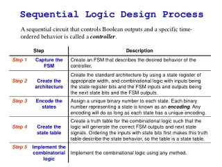
General FSM design procedure • (1) Determine inputs and outputs • (2) Determine possible states of machine • state minimization • (3) Encode states and outputs into a binary code • state assignment or state encoding • output encoding • possibly input encoding (if under our control) • (4) Realize logic to implement functions for states and outputs • combinational logic implementation and optimization • choices in steps 2 and 3 can have large effect on resulting logic Contemporary Logic Design
Finite string pattern recognizer (step 1) • Finite string pattern recognizer • one input (X) and one output (Z) • output is asserted whenever the input sequence …010… has been observed, as long as the sequence …100… has never been seen • Step 1: understanding the problem statement • sample input/output behavior: X: 0 0 1 0 1 0 1 0 0 1 0 … Z: 0 0 0 1 0 1 0 1 0 0 0 … X: 1 1 0 1 1 0 1 0 0 1 0 … Z: 0 0 0 0 0 0 0 1 0 0 0 … Contemporary Logic Design
reset S0[0] 0 1 S1 [0] S4[0] 1 0 S2 [0] S5[0] 0 0 S3 [1] S6[0] 0 or 1 Finite string pattern recognizer (step 2) • Step 2: draw state diagram • for the strings that must be recognized, i.e., 010 and 100 • a Moore implementation Contemporary Logic Design
reset S0[0] 0 1 0 S1 [0] S4[0] 1 ...0 ...1 1 0 S2 [0] S5[0] ...01 0 1 0 S3 [1] S6[0] 0 or 1 ...010 ...100 Finite string pattern recognizer (step 2, cont’d) • Exit conditions from state S3: have recognized …010 • if next input is 0 then have …0100 = ...100 (state S6) • if next input is 1 then have …0101 = …01 (state S2) • Exit conditions from S1: recognizesstrings of form …0 (no 1 seen) • loop back to S1 if input is 0 • Exit conditions from S4: recognizesstrings of form …1 (no 0 seen) • loop back to S4 if input is 1 Contemporary Logic Design
0 1 ...0 ...1 1 1 ...10 Finite string pattern recognizer (step 2, cont’d) • S2 and S5 still have incomplete transitions • S2 = …01; If next input is 1,then string could be prefix of (01)1(00) S4 handles just this case • S5 = …10; If next input is 1,then string could be prefix of (10)1(0) S2 handles just this case • Reuse states as much as possible • look for same meaning • state minimization leads tosmaller number of bits torepresent states • Once all states have a completeset of transitions we have afinal state diagram reset S0[0] 0 1 S1 [0] S4[0] 1 0 S2 [0] S5[0] ...01 0 1 0 S3 [1] S6[0] 0 or 1 ...010 ...100 Contemporary Logic Design
Finite string pattern recognizer (step 3) • Verilog description including state assignment (or state encoding) module string (clk, X, rst, Q0, Q1, Q2, Z); input clk, X, rst; output Q0, Q1, Q2, Z; parameter S0 = [0,0,0]; //reset stateparameterS1 = [0,0,1]; //strings ending in ...0parameterS2 = [0,1,0]; //strings ending in ...01parameterS3 = [0,1,1]; //strings ending in ...010parameterS4 = [1,0,0]; //strings ending in ...1parameterS5 = [1,0,1]; //strings ending in ...10parameterS6 = [1,1,0]; //strings ending in ...100 reg state[0:2]; assign Q0 = state[0]; assign Q1 = state[1]; assign Q2 = state[2]; assign Z = (state == S3); always @(posedge clk) begin if (rst) state = S0; else case (state) S0: if (X) state = S4 else state = S1; S1: if (X) state = S2 else state = S1; S2: if (X) state = S4 else state = S3; S3: if (X) state = S2 else state = S6; S4: if (X) state = S4 else state = S5; S5: if (X) state = S2 else state = S6; S6: state = S6; default: begin $display (“invalid state reached”); state = 3’bxxx; end endcase end endmodule Contemporary Logic Design
Finite string pattern recognizer • Review of process • understanding problem • write down sample inputs and outputs to understand specification • derive a state diagram • write down sequences of states and transitions for sequences to be recognized • minimize number of states • add missing transitions; reuse states as much as possible • state assignment or encoding • encode states with unique patterns • simulate realization • verify I/O behavior of your state diagram to ensure it matches specification Contemporary Logic Design
Implementation • Implementation • NS0 = CS0Q2’ + CS2’X + CS1CS2X’ + CS0X’ • NS1 = CS1X’ + CS0CS2 + CS0CS1 + CS2X • NS2 = CS0’CS2’X’ + CS1’CS2’X’ + CS0’CS1’X’ • Z = CS0’CS1CS2 P010 P100 Reset R D Q R D Q X Clk Contemporary Logic Design
Reset S0 [0] P010 P100 P’010 P’100 S1 [1] S2 [0] P100 P010 Minimization • Minimization • NS0 = CS0 + P100 • NS1 = CS0’P010 + CS1P010 = CS0’P010 • Z = CS1 Contemporary Logic Design
P010 P100 Reset R D Q R D Q R D Q X Clk R D Q Finite String Pattern Recognizer • Complete circuit Contemporary Logic Design
Mode Input M 0 0 1 1 1 0 0 Current State 000 001 010 110 111 101 110 Next State 001 010 110 111 101 110 111 Complex counter • A synchronous 3-bit counter has a mode control M • when M = 0, the counter counts up in the binary sequence • when M = 1, the counter advances through the Gray code sequence binary: 000, 001, 010, 011, 100, 101, 110, 111 Gray: 000, 001, 011, 010, 110, 111, 101, 100 • Valid I/O behavior (partial) Contemporary Logic Design
0 S0[000] S1[001] S2[010] S3[011] S4[100] S5[101] S6[110] S7[111] 1 reset 0 0 0 0 0 0 0 1 1 1 1 1 1 1 Complex counter (state diagram) • Deriving state diagram • one state for each output combination • add appropriate arcs for the mode control Contemporary Logic Design
Complex counter (state encoding) • Verilog description including state encoding module string (clk, M, rst, Z0, Z1, Z2); input clk, X, rst; output Z0, Z1, Z2; parameter S0 = [0,0,0]; parameterS1 = [0,0,1]; parameterS2 = [0,1,0]; parameterS3 = [0,1,1]; parameterS4 = [1,0,0]; parameterS5 = [1,0,1]; parameterS6 = [1,1,0]; parameterS7 = [1,1,1]; reg state[0:2]; assign Z0 = state[0]; assign Z1 = state[1]; assign Z2 = state[2]; always @(posedge clk) begin if rst state = S0; else case (state) S0: state = S1; S1: if (M) state = S3 else state = S2; S2: if (M) state = S6 else state = S3; S3: if (M) state = S2 else state = S4; S4: if (M) state = S0 else state = S5; S5: if (M) state = S4 else state = S6; S6: if (M) state = S7 else state = S7; S7: if (M) state = S5 else state = S0; endcase end endmodule Contemporary Logic Design
TS' S1a S1 TS/ST S1b S1c –/ST Traffic light controlleras two communicating FSMs • Without separate timer • S0 would require 7 states • S1 would require 3 states • S2 would require 7 states • S3 would require 3 states • S1 and S3 have simple transformation • S0 and S2 would require many more arcs • C could change in any of seven states • By factoring out timer • greatly reduce number of states • 4 instead of 20 • counter only requires seven or eight states • 12 total instead of 20 traffic light controller ST TS TL timer Contemporary Logic Design
Traffic light controller FSM • Specification of inputs, outputs, and state elements module FSM(HR, HY, HG, FR, FY, FG, ST, TS, TL, C, reset, Clk); output HR; output HY; output HG; output FR; output FY; output FG; output ST; input TS; input TL; input C; input reset; input Clk; reg [6:1] state; reg ST; parameter highwaygreen = 6'b001100; parameterhighwayyellow = 6'b010100; parameterfarmroadgreen = 6'b100001; parameterfarmroadyellow = 6'b100010; assign HR = state[6]; assign HY = state[5]; assign HG = state[4]; assign FR = state[3]; assign FY = state[2]; assign FG = state[1]; specify state bits and codes for each state as well as connections to outputs Contemporary Logic Design
Traffic light controller FSM (cont’d) initial begin state = highwaygreen; ST = 0; end always @(posedge Clk) begin if (reset) begin state = highwaygreen; ST = 1; end else begin ST = 0; case (state) highwaygreen: if (TL & C) begin state = highwayyellow; ST = 1; end highwayyellow: if (TS) begin state = farmroadgreen; ST = 1; end farmroadgreen: if (TL | !C) begin state = farmroadyellow; ST = 1; end farmroadyellow: if (TS) begin state = highwaygreen; ST = 1; end endcase end endendmodule case statementtriggerred byclock edge Contemporary Logic Design
Timer for traffic light controller • Another FSM module Timer(TS, TL, ST, Clk); output TS; output TL; input ST; input Clk; integer value; assign TS = (value >= 4); // 5 cycles after reset assign TL = (value >= 14); // 15 cycles after reset always @(posedge ST) value = 0; // async reset always @(posedge Clk) value = value + 1;endmodule Contemporary Logic Design
Complete traffic light controller • Tying it all together (FSM + timer) • structural Verilog (same as a schematic drawing) module main(HR, HY, HG, FR, FY, FG, reset, C, Clk); output HR, HY, HG, FR, FY, FG; input reset, C, Clk; Timer part1(TS, TL, ST, Clk); FSM part2(HR, HY, HG, FR, FY, FG, ST, TS, TL, C, reset, Clk);endmodule traffic light controller ST TS TL timer Contemporary Logic Design
X CLKFSM1XFSM2Y FSM 1 FSM 2 Y A A B C D D X==0 Y==0 Y==0 X==0 C[0] A[1] X==1 Y==1 D[1] B[0] X==0 X==1 Communicating finite state machines • One machine's output is another machine's input machines advance in lock step initial inputs/outputs: X = 0, Y = 0 Contemporary Logic Design
Data-path and control • Digital hardware systems = data-path + control • datapath: registers, counters, combinational functional units (e.g., ALU), communication (e.g., busses) • control: FSM generating sequences of control signals that instructs datapath what to do next "puppeteer who pulls the strings" control status info and inputs control signal outputs state data-path "puppet" Contemporary Logic Design
Digital combinational lock • Door combination lock: • punch in 3 values in sequence and the door opens; if there is an error the lock must be reset; once the door opens the lock must be reset • inputs: sequence of input values, reset • outputs: door open/close • memory: must remember combination or always have it available • open questions: how do you set the internal combination? • stored in registers (how loaded?) • hardwired via switches set by user Contemporary Logic Design
Implementation in software • integer combination_lock ( ) { • integer v1, v2, v3; • integer error = 0; • static integer c[3] = 3, 4, 2; • while (!new_value( )); • v1 = read_value( ); • if (v1 != c[1]) then error = 1; • while (!new_value( )); • v2 = read_value( ); • if (v2 != c[2]) then error = 1; • while (!new_value( )); • v3 = read_value( ); • if (v2 != c[3]) then error = 1; • if (error == 1) then return(0); else return (1); • } Contemporary Logic Design
new value reset clock open/closed Determining details of the specification • How many bits per input value? • How many values in sequence? • How do we know a new input value is entered? • What are the states and state transitions of the system? Contemporary Logic Design
Digital combination lock state diagram • States: 5 states • represent point in execution of machine • each state has outputs • Transitions: 6 from state to state, 5 self transitions, 1 global • changes of state occur when clock says its ok • based on value of inputs • Inputs: reset, new, results of comparisons • Output: open/closed ERR closed C1!=value& new C2!=value& new C3!=value& new S1 S2 S3 OPEN reset closed closed closed open C1==value& new C2==value& new C3==value& new not new not new not new Contemporary Logic Design
new reset C1 C2 C3 4 4 4 mux control multiplexer 4 controller clock value comparator equal 4 open/closed Data-path and control structure • Data-path • storage registers for combination values • multiplexer • comparator • Control • finite-state machine controller • control for data-path (which value to compare) Contemporary Logic Design
next reset new equal state state mux open/closed1 – – – S1 C1 closed0 0 – S1 S1 C1 closed0 1 0 S1 ERR – closed0 1 1 S1 S2 C2 closed...0 1 1 S3 OPEN – open... State table for combination lock • Finite-state machine • refine state diagram to take internal structure into account • state table ready for encoding Contemporary Logic Design
new reset mux control controller clock equal next open/closed reset new equal state state mux open/closed1 – – – 0001 001 00 0 – 0001 0001 001 00 1 0 0001 0000 – 00 1 1 0001 0010 010 0...0 1 1 0100 1000 – 1... Encodings for combination lock • Encode state table • state can be: S1, S2, S3, OPEN, or ERR • needs at least 3 bits to encode: 000, 001, 010, 011, 100 • and as many as 5: 00001, 00010, 00100, 01000, 10000 • choose 4 bits: 0001, 0010, 0100, 1000, 0000 • output mux can be: C1, C2, or C3 • needs 2 to 3 bits to encode • choose 3 bits: 001, 010, 100 • output open/closed can be: open or closed • needs 1 or 2 bits to encode • choose 1 bit: 1, 0 mux is identical to last 3 bits of stateopen/closed is identical to first bit of state therefore, we do not even need to implement FFs to hold state, just use outputs Contemporary Logic Design
value C1i C2i C3i mux control C1 C2 C3 4 4 4 mux control multiplexer 4 value comparator equal 4 equal Data-path implementationfor combination lock • Multiplexer • easy to implement as combinational logic when few inputs • logic can easily get too big for most PLDs Contemporary Logic Design
C1 C2 C3 4 4 4 mux control multiplexer 4 value comparator equal 4 Data-path implementation (cont’d) • Tri-state logic • utilize a third output state: “no connection” or “float” • connect outputs together as long as only one is “enabled” • open-collector gates canonly output 0, not 1 • can be used to implementlogical AND with only wires value C1i C2i C3i mux control + oc tri-state driver (can disconnectfrom output) equal open-collector connection (zero whenever one connection is zero, one otherwise – wired AND) Contemporary Logic Design
In OE OutX 0 Z0 1 01 1 1 Tri-state gates • The third value • logic values: “0”, “1” • don't care: “X” (must be 0 or 1 in real circuit!) • third value or state: “Z” — high impedance, infinite R, no connection • Tri-state gates • additional input – output enable (OE) • output values are 0, 1, and Z • when OE is high, the gate functions normally • when OE is low, the gate is disconnected from wire at output • allows more than one gate to be connected to the same output wire • as long as only one has its output enabled at any one time (otherwise, sparks could fly) OE In Out 100 non-inverting tri-statebuffer In OE Out Contemporary Logic Design
F Input0 OE Input1 OE Select Tri-state and multiplexing • When using tri-state logic • (1) make sure never more than one "driver" for a wire at any one time (pulling high and low at the same time can severely damage circuits) • (2) make sure to only use value on wire when its being driven (using a floating value may cause failures) • Using tri-state gates to implement an economical multiplexer when Select is highInput1 is connected to F when Select is lowInput0 is connected to F this is essentially a 2:1 mux Contemporary Logic Design
Open-collector gates and wired-AND • Open collector: another way to connect gate outputs to the same wire • gate only has the ability to pull its output low • it cannot actively drive the wire high (default – pulled high through resistor) • Wired-AND can be implemented with open collector logic • if A and B are "1", output is actively pulled low • if C and D are "1", output is actively pulled low • if one gate output is low and the other high, then low wins • if both gate outputs are "1", the wire value "floats", pulled high by resistor • low to high transition usually slower than it would have been with a gate pulling high • hence, the two NAND functions are ANDed together with ouputs wired together using "wired-AND"to form (AB)'(CD)' open-collector NAND gates Contemporary Logic Design
ld1 ld2 ld3 C1 C2 C3 4 4 4 mux control multiplexer 4 value comparator equal 4 Digital combination lock (new data-path) • Decrease number of inputs • Remove 3 code digits as inputs • use code registers • make them loadable from value • need 3 load signal inputs (net gain in input (4*3)–3=9) • could be done with 2 signals and decoder(ld1, ld2, ld3, load none) Contemporary Logic Design
Transmitter/Receiver • RS-232 protocol for formatting the data on the wire • It is assumed that the wire is normally high (quiescent value) • Start bit • Stop bit 8 Data Bits Stop Bit Start Bit Contemporary Logic Design
Transmitter/Receiver Block diagram of serial line transmitter/receiver Schematic diagram of a keyboard block with debouncing circuitry Contemporary Logic Design
Transmitter/Receiver Schematic diagram of a single keyboard key Four-cycle handshake with data Contemporary Logic Design
Hold Time Setup Time E (data bit) DB Valid Data RS Valid Mode Transmitter/Receiver Timing of LCD screen interface LCD screen operation • Display Contemporary Logic Design
Transmitter/Receiver • Detailed timing for the receiver part of our circuit Contemporary Logic Design
Section summary • FSM design • understanding the problem • generating state diagram • communicating state machines • Four case studies • understand I/O behavior • draw diagrams • enumerate states for the "goal" • expand with error conditions • reuse states whenever possible Contemporary Logic Design