Sequential Logic Design in Digital Systems
Explore flight attendant call-button systems, SR latches, D flip-flops, clock signals, and more concepts in sequential logic design. Learn about storage blocks, latches vs. flip-flops, edge-triggered circuits, and FSMs for efficient digital designs.

Sequential Logic Design in Digital Systems
E N D
Presentation Transcript
Digital Design - Sequential Logic Design Chapter 3 - Sequential Logic Design
Digital DesignSequential Logic Design Figure 3.1 Flight-attendant call-button system. Pressing Call turns on the light, which stays on after Call is released. Pressing Cancel turns off the light.
Digital DesignSequential Logic Design Figure 3.2 First (failed) attempt at using feedback to store a bit. Figure 3.3 Tracing the behavior of our first attempt at bit storage.
Digital DesignSequential Logic Design Figure 3.5 SR latch when S=0 and R=1 Figure 3.4 Basic SR Latch Figure 3.6 SR latch when S=0 and R=0
Digital DesignSequential Logic Design Figure 3.7 SR latch when S=1 and R=0 Figure 3.4 Basic SR Latch Figure 3.8 SR latch when S=0 and R=0
Digital DesignSequential Logic Design Figure 3.9 Flight attendant call-button system using a basic SR latch.
Digital DesignSequential Logic Design Figure 3.10 S=1 and R=1 causes problems -- Q oscillates. Figure 3.11 Q eventually settles to either 0 or 1, due to race condition.
Digital DesignSequential Logic Design Figure 3.12 Conceptually, S and R can’t both be 1 in this sample circuit. But in reality, they can, due to the delay of the inverter and AND gate. Figure 3.13 Gate delays can cause SR=11.
Digital DesignSequential Logic Design Figure 3.14/3.15 Level-sensitive SR latch -- an SR latch with enable input C.
Digital DesignSequential Logic Design Figure 3.16 Symbol for dual-output level-sensitive SR latch.
Digital DesignSequential Logic Design Figure 3.17 An example of a clock signal named Clk. Circuit inputs should only change while Clk=0, such that latch inputs will be stable when Clk=1.
Digital DesignSequential Logic Design Figure 3.20 A problem with latches -- through how many latches will Y propoagate for each pulse of Clk_A? For Clk_B? Figure 3.18 D latch. Figure 3.19 D latch symbol.
Digital DesignSequential Logic Design Figure 3.21 A problem with level-sensitive latches
Digital DesignSequential Logic Design Figure 3.23 A D flip-flop implementing an edge-triggered bit storage block, internally using two latches in a master-slave arrangement.
Digital DesignSequential Logic Design Figure 3.24 Using D flip-flops, we now know through how many flip-flops Y will propagate for Clk_A and for Clk_B -- one flip-flop exactly per pulse, for either clock signal.
Digital DesignSequential Logic Design Figure 3.25 Positive (shown on the left) and negative (right) edge-triggered D flip-flops. The sideways triangle input represents an edge-triggered clock input.
Digital DesignSequential Logic Design Figure 3.26 Latch versus flip-flop timing.
Digital DesignSequential Logic Design Figure 3.27 Flight attendant call-button system using a D flip-flop. Table 3.1 D truth table for call-button system.
Digital DesignSequential Logic Design D flip-flop Level-sensitiveSR latch SR latch D latch D S (set) S S S1 D latch D latch D Q’ Qs’ Dm Qm Ds C C Q Cm Cs Qs Q Q Q master slave R Clk R R (reset) R1 : SR can’t be 11 Feature: Only loads D Feature : S=1 sets Feature : S and R only Feature if D is stable before and value present at rising Q to 1, R=1 have effect when C=1. while C=1, and will be clock edge, so values resets Q to 0. We can design outside 11 for only a brief glitch can’t propagate to other : SR=11 Problem circuit so SR=11 even if D changes while flip-flops during same yield undefined never happens when C=1. : C=1 too clock cycle. : Problem Tradeoff Q. C=1. : Problem long propagates new uses more gates avoiding SR=11 can values through too many internally than D latch, be a burden. latches; too short may and requires more not enable a store. external gates than SR-- but gate count is less of an issue today. Figure 3.28 Increasingly-better bit storage blocks, leading to the D flip-flop.
Digital DesignSequential Logic Design Figure 3.29 A basic 4-bit register internal design (left) and block symbol (right).
Digital DesignSequential Logic Design Figure 3.30 Temperature history display system. Figure 3.31 Internal design of the TemperatureHistoryStorage component.
Digital DesignSequential Logic Design Figure 3.32 Example of values in the TemperatureHistoryStorage registers. One particular data item, 18, is shown moving through the registers on each clock cycle.
Digital DesignSequential Logic Design Figure 3.33 Laser Timer System Figure 3.34 First (bad) attempt to implement the laser surgery system.
Digital DesignSequential Logic Design Figure 3.35 A simple state diagram (left) and the timing diagram describing the state diagram’s behavior (right).
Digital DesignSequential Logic Design Figure 3.36 Three-cycles-high system: state diagram (left), timing diagram (right).
Digital DesignSequential Logic Design Figure 3.37 Three-cycles-high system: state diagram (left), timing diagram (right).
Digital DesignSequential Logic Design • Finite-state machine, or FSM, consists of several things: • A set of states. Our example had four states: {On1, On2, On3, Off}. • A set of inputs, and a set of outputs. Our example had one input: {b}, and one output: {x}. • An initial state, namely, a state to start in when we power up the system. Our example’s initial state was Off. • A description of the next state to go to based on the current state and the values of the inputs. Our example used directed edges with associated input conditions to tell us the next state. Those edges with conditions are known as transitions. • A description of what output values to generate in each state. Our example assigns a value to x in every state. Assigning an output in an FSM is known as an action.
Digital DesignSequential Logic Design Figure 3.38 Laser timer state diagram assuming every transition is ANDed with a rising clock.
Digital DesignSequential Logic Design Figure 3.39 Why are the heads of keys getting thicker? Note that the key on the right is thicker than the key on the left. The key on the right has a computer chip inside that sends an identifier to the car’s computer, thus helping to reduce car thefts.. Figure 3.40 Secure car key FSM. Figure 3.41 Secure car key timing diagram.
Digital DesignSequential Logic Design Figure 3.44 Code detector FSM.
Digital DesignSequential Logic Design Figure 3.45 Improved code detector FSM.
Digital DesignSequential Logic Design Figure 3.46 Standard controller architecture for the laser timer.
s M o t Combinational I O F u u S t S p F p logic n u M i t s S clk State register N Digital DesignSequential Logic Design Figure 3.47 Standard controller architecture -- general view.
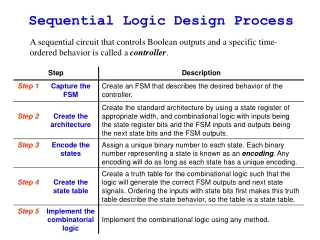
Digital DesignSequential Logic Design Table 3.2 Five-step process for designing a controller.
Combinational I O FSM Inputs FSM Outputs logic S N clk State register Digital DesignSequential Logic Design Step 1: Capture the FSM Step 2: Create the architecture Example: Three-cycles-high laser timer controller.
Digital DesignSequential Logic Design Step 3: Encode the states Step 4: Create the state table Example: Three-cycles-high laser timer controller.
Digital DesignSequential Logic Design Step 5: Implement the combinational logic Example: Three-cycles-high laser timer controller.
Digital DesignSequential Logic Design Figure 3.50 Tracing the behavior of the three-cycles-high laser timer controller.
Digital DesignSequential Logic Design Figure 3.51 Desired timing diagram of the button press synchronizer.
Digital DesignSequential Logic Design Figure 3.52 Button press synchronizer design steps: (a) initial FSM, (b) architecture, (c) FSM with encoded states, (d) state table, (e) final circuit with implemented combinational logic.
Digital DesignSequential Logic Design Step 1: Capture the FSM Step 2: Create the architecture Figure 3.53 Sequence generator FSM. Figure 3.54 Sequence generator controller architecture.
Digital DesignSequential Logic Design • Step 3: Encode the states • A: 00, B: 01, C: 10, D: 11 • Step 4: Create the state table • Step 5: Implement the combinational logic Figure 3.55 Sequence generator controller architecture.
Digital DesignSequential Logic Design Step 1: Capture the FSM Step 2: Create the architecture Figure 3.40 Secure car key FSM. Figure 3.56 Secure car key controller architecture.
Digital DesignSequential Logic Design • Step 3: Encode the states • Step 4: Create the state table
Digital DesignSequential Logic Design Figure 3.58 Setup time violation.
Digital DesignSequential Logic Design Figure 3.59 D flip-flop with asynchronous reset AR (left), and with asychronous set (right). Figure 3.60 Asynchronous reset forces the flip-flop to 0, independent of clk or D.
Digital DesignSequential Logic Design Figure 3.61 Three-cycles-high laser timer controller with a reset input that loads the state register with the initial state 00.
Digital DesignSequential Logic Design Figure 3.62 Pacemaker with leads (left), and pacemaker’s location under the skin (right). Courtesy of Medtronic, Inc. Figure 3.63 A basic pacemaker’s controller FSM.
Digital DesignSequential Logic Design Figure 3.64 An atrioventricular pacemaker’s controller FSM (using the convention that FSM outputs not explicitly set in a state are implicitly set to 0).