Download
1 / 2
20 likes | 131 Views
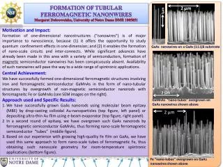
2 µm. FORMATION OF TUBULAR FERROMAGNETIC NANONWIRES Margaret Dobrowolska , University of Notre Dame DMR 1005851. 1µm. Motivation and Impact:

E N D
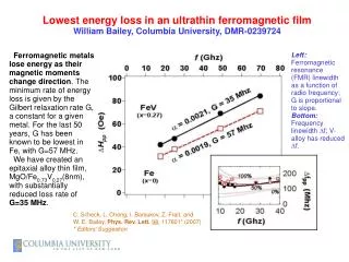
2 µm FORMATION OF TUBULAR FERROMAGNETIC NANONWIRES Margaret Dobrowolska, University of Notre Dame DMR 1005851 1µm Motivation and Impact: Formation of one-dimensional nanostructures (“nanowires”) is of major importance to nanoscience, because (1) it offers the opportunity to study quantum confinement effects in one-dimension; and (2) it enables the formation of nano-scale circuits and inter-connects. While significant advances have already been made in this area with a variety of semiconductors, formation of magnetic semiconductor nanowires has been conspicuously absent. Availability of such nanowires will pave the way to a wide range of spintronic applications. Central Achievement: We have successfully formed one-dimensional ferromagnetic structures involving iron and ferromagnetic semiconductor GaMnAs in the form of nano-tubular structures by overgrowth of non-magnetic semiconductor nanorods with ferromagneitc Fe or GaMnAs (see SEM images on the right). Approach used and Specific Results: We have successfully grown GaAsnanorodsusing molecular beam epitaxy (MBE) by drop-casting colloidal Au-nanoparticles (top figure, left panel) or depositing ultra-thin Au film using e-beam evaporator (top figure, right panel). In a second round of epitaxy, we have overgrown such GaAsnanorods by ferromagnetic semiconductor GaMnAs, thus forming nano-scale ferromagnetic semiconductor “tubes” (middle figure). 3. Based on our experience with growing high-quality Fe film on GaAs, we have used this same approach to form nano-scale tubes of ferromagnetic Fe, thus obtaining such nanoscale geometry for room-temperature spintronic applications (bottom figure). • GaAs nanowires on a GaAs(111)B substrate 2 µm • GaMnAs “nano-tubes” overgrown on • GaAsnanowires shown above 2 µm • Fe “nano-tubes” overgrown on GaAsnanowires shown above
Broader Impact Margaret Dobrowolska, University of Notre Dame DMR 1005851 Our program typically involvesfour graduate students and two undergraduate students each year. Our program exposes these students to a wide range of materials fabrication and characterization techniques, thus preparing them for the US manpower needs in the area of semiconductor science and technology. We also conduct a broad program of international scientific exchanges. As an illustration, we are hosting Prof. Sanghoon Lee from Korea University for a one-year visit; and in May 2011 we have hosted Dr. A. Scherbakov from the Ioffe Institute, St. Petersburg, Russia for a one-month visit. One of our graduate students, Joe Hagmann (seen here with Dr. In-Ho Kim, Director of NRF’s Division of Global Networking) conducted his research at Korea University in the Summer of 2010 as an NSF-EAPSI Fellow. This represents a long-term relationship: another of our graduate students, Mr. Jon Leiner, has similarly spent the Summer of 2009 at Korea University as an NSF-EAPSI Fellow; and their host, Prof. S. Lee, is currently spending his sabbatical at Notre Dame. Societal Impact: Our group has been continually active as a resource of materials for other groups. We are currently interacting with at least 20 other institutions by providing them with magnetic semiconductor specimens for their research. The understanding of these materials and of their heterostructures obtained in our laboratory is thus automatically of benefit to our collaborators (including their graduate students), whose research depends not only on the specimens that we provide, but on the intellectual input from our group in the form of characterization and general understanding of the properties of these materials.