Download
1 / 31
520 likes | 996 Views
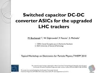
Switched capacitor DC-DC converter ASICs for the upgraded LHC trackers. M. Bochenek 1,2 , W . Dąbrowski 2 , F. Faccio 1 , S. Michelis 1. 1. CERN , Conseil Européen pour la Recherche Nucléaire 2. AGH , University of Science & Technology.

E N D
Switched capacitor DC-DC converter ASICs for the upgraded LHC trackers M. Bochenek1,2, W. Dąbrowski2, F. Faccio1, S. Michelis1 1. CERN, Conseil Européen pour la Recherche Nucléaire 2. AGH, University of Science & Technology Topical Workshop on Electronics for Particle Physics, TWEPP 2010 This research project has been supported by a Marie Curie Initial Training Network Fellowship of the European Community’s & Seventh Framework Programme under contract number (PITN-GA-2008-211801-ACEOLE) This project has received funding from the European Community's Seventh Framework Programme (FP7/2007-2013) under project SLHC-PP, Grant Agreement no 212114. ACEOLE
Outline 1. Powering schemes considered for upgraded ATLAS Inner Tracker 2. Switched capacitor step-down converter proposed for the DC-DC powering scheme • A model of a simple step-down (2:1) converter and its practical implementation, • Designs of the non-overlapping clock generator and buffers. 3. Switched capacitor voltage doubler proposed for the serial powering scheme • A model of a simple voltage doubler and its practical implementation, • Designs of the non-overlapping clock generator, level shifters and buffers. Due to the fact that the IBM 0.13 µm submission was delayed, we have to wait for the results from the chips.
1. Overview of the powering schemes considered for the upgraded ATLAS Inner Tracker
Serial powering scheme Good quality of analog and digital voltage: • low output impedance of shunt regulator, • possibility to use classical linear regulator → good filtering efficiency. No regulation on DC-DC, but the power consumption in the analog part is constant.
DC-DC conversion technique • A low-dropout voltage regulator in the “analog bus” is required. • No regulation on the digital power line (required low impedance of DC-DC since the current consumption varies significantly in the digital part).
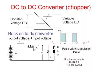
A simple model of the step-down switched capacitor converter • Phase 1: • Switches S1 and S3 are closed, • Switches S2 and S4 are opened, • CX and CL are connected in series. • The simplest model for • the 2:1 converter contains: • Four switches • Two capacitors • Phase 2: • Switches S1 and S3 are opened, • Switches S2 and S4 are closed, • CXand CL are connected in parallel.
Types of losses in switching MOSFETs The optimization process is based on minimizing the contradictory types of losses in the switching MOSFETs • Conduction losses ( equal to: I2 • R ) – therefore the total resistance between the source and drain during the “ON” state, RDS(on) has to be as low as possible, • Switching losses ( equal to: ts• VDS • I • f ) – switching time, rise and fall time depend on the gate to drain capacitance CGD, internal resistance of the driver and the VTH, • Gate charge losses ( equal to: f • QG(TOT)• VDRIVE) – are caused by charging up the gate capacitance and then dumping the charge to ground every cycle.
Practical solution for the DC-DC step-down converter Power Efficiency = 97% • VDD= 1.9 V • VOUT= 926 mV • IOUT = 60 mA • CX= 1000 nF • CL= 200 nF • f= 1 MHz (including all circuitry)
Schematic diagram of the non-overlapping clock generator used in the step-down converter 3.5 ns 2 x NOR gate 3 x inverter 2 x current starved inverter C1 = C2 = 20 fF allows for a clock signal separation of 3.5ns 3.5 ns
Buffer used in the step-down converter M1 M3 M4 M2 Top Two chains of scaled inverters with cross-coupled transistors M1 and M2 allow to avoid the conduction current in the last inverter M3 / M4 This architecture of the buffer was used by S. Michelis in AMIS2 Bottom
Layout of the step-down converter M1 = 28.2 mm / 0.24 µm, M2 = M3 = 18.0 mm / 0.30 µm, M4 = 6.0 mm / 0.30 µm Clock generator M4 buffer M2 buffer M3 buffer M1 buffer 200 µm M3 (NFET) M2 (NFET) M4 (NFET) M1 (PFET) 580 µm Total area = 0.12 mm2
Simulation cell for the transient analysis (including package components)
Time response of the step-down converter (no wire bonds) 17mV
Time response of the step-down (wire bond inductance included) Vpp = 150 mV (for L=1nH)
Power efficiency and output voltage vs. output current The converter was optimized for IOUT=60 mA
A simple model of the step-up switched capacitor converter • Phase 1: • Switches S1 and S3 are closed, • Switch S2 is opened, • Capacitor is charged to the • supply voltage VDD • A simple model contains: • Three switches • One capacitor • Phase 2: • Switches S1 and S3 are opened, • Switch S2 is closed, • Bottom plate of the capacitor on VDD, • while the capacitor maintains its charge • VDDC (from the previous phase).
Practical solution for the voltage doubler • VDD= 0.9 V • VOUT= 1.55 V • IOUT= 32 mA • CPUMP= 470 nF • CLOAD= 470 nF • f= 500 kHz M1, M2 = 980 μm / 0.15 μm M3, M4 = 2000 μm / 0.24 μm M5, M6 = 10 μm / 0.24 μm 1.5 V NFETs 2.5V PFETs Power Efficiency = 85% (including all circuitry)
Level shifter Because of poor driving capability of used big PMOS serial switches two level shifters are needed The level shifter requires two voltage supply domains: input voltage supply (0.9 V) and output supply (1.6 V) - taken from the output of the charge pump
Layout of the charge pump Buffers Voltage Doubler Level Shifters 190 µm Clock Generator Total area = 0.04 mm2 200 µm
Simulation cell for the transient analysis (including package components)
Time response of the step-up (wire bond inductance included) Vpp = 900 mV (for L=1nH)
Power efficiency and output voltage vs. output current The converter was optimized for IOUT = 30mA
Layout of the DCDC013 2x Step-up Converter 2 mm 2x Step-down Converter 2 mm
Conclusions • The results from the Spectre simulations are quite promising: - η = 97% for the step-down converter, - η = 85% for the step-up converter. • The inductance of the bond wires causes fast voltage spikes – the padring was designed to reduce the influence of the bond wire inductance. Therefore, the use of the DC-DC converters mounted on the separate chip with C4 pads should be considered. • The chip was submitted at the end of August 2010. • The PCB board is now in production and will be ready before the arrival of the chips.
Thank you! This research project has been supported by a Marie Curie Initial Training Network Fellowship of the European Community’s & Seventh Framework Programme under contract number (PITN-GA-2008-211801-ACEOLE) This project has received funding from the European Community's Seventh Framework Programme (FP7/2007-2013) under project SLHC-PP, Grant Agreement no 212114. ACEOLE
Backup 3.5 ns