ENE 311
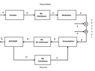
ENE 311. Lecture 6. Donors and Acceptors. We have learned how to find new position of Fermi level for extrinsic semiconductors. Now let us consider the new electron density in case of both donors N D and acceptors N A are present simultaneously.


ENE 311
E N D
Presentation Transcript
ENE 311 Lecture 6
Donors and Acceptors • We have learned how to find new position of Fermi level for extrinsic semiconductors. • Now let us consider the new electron density in case of both donors ND and acceptors NA are present simultaneously. • The Fermi level will adjust itself to preserve overall charge neutrality as (1)
Donors and Acceptors • By solving (1) with , the equilibrium electron and hole concentrations in an n-type semiconductors yield
Donors and Acceptors • Similarly to p-type semiconductors, the electron and hole concentrations are expressed as
Donors and Acceptors • Generally, in case of all impurities are ionized, the net impurity concentration ND – NA is larger than the intrinsic carrier concentration ni; therefore, we may simply rewrite the above relationship as
Donors and Acceptors • The figure shows electron density in Si as a function of temperature for a donor concentration of ND = 1015 cm-3. • At low temperature, not all donor impurities could be ionized and this is called “Freeze-out region” since some electrons are frozen at the donor level.
Donors and Acceptors • As the temperature increased, all donor impurities are ionized and this remains the same for a wide range of temperature. • This region is called “Extrinsic region”.
Donors and Acceptors • Until the temperature is increased even higher and it reaches a point where electrons are excited from valence band. • This makes the intrinsic carrier concentration becomes comparable to the donor concentration. • At this region, the semiconductors act like an intrinsic one.
Donors and Acceptors • If the semiconductors are heavily doped for both n- or p-type, EF will be higher than EC or below EV, respectively. • The semiconductor is referred to as degeneratesemiconductor. • This also results in the reduction of the bandgap.
Donors and Acceptors • This also results in the reduction of the bandgap. The bandgap reduction Eg for Si at room temperature is expressed by where the doping is in the unit of cm-3.
Donors and Acceptors • Ex. Si is doped with 1016 arsenic atoms/cm3. Find the carrier concentration and the Fermi level at room temperature (300K).
Donors and Acceptors Soln At room temperature, complete ionization of impurity atoms is highly possible, then we have n = ND = 1016 cm-3.
Donors and Acceptors Soln The Fermi level measured from the bottom of the conduction band is
Donors and Acceptors Soln The Fermi level measured from the intrinsic Fermi level is
Direct Recombination • When a bond between neighboring atoms is broken, an electron-hole pair is generated. • The valence electron moves upward to the conduction band due to getting thermal energy. • This results in a hole being left in the valence band.
Direct Recombination • This process is called carrier generation with the generation rate Gth (number of electron-hole pair generation per unit volume per time). • When an electron moves downward from the conduction band to the valence band to recombine with the hole, this reverse process is called recombination. • The recombination rate represents by Rth.
Direct Recombination • Under thermal equilibrium, the generation rate Gth equals to the recombination rate Rth to preserve the condition of • The direct recombination rate R can be expressed as where is the proportionality constant.
Direct Recombination • Therefore, for an n-type semiconductor, we have (3) where nn0 and pn0 represent electron and hole densities at thermal equilibrium.
Direct Recombination • If the light is applied on the semiconductor, it produces electron-hole pairs at a rate GL, the carrier concentrations are above their equilibrium values. • The generation and recombination rates become where n and p are the excess carrie concentrations
Direct Recombination • n = p to maintain the overall charge neutrality. • The net rate of change of hole concentration is expressed as (7)
Direct Recombination • In steady-state, dpn/dt = 0. From (7) we have (8) where U is the net recombination rate. Substituting (3) and (5) into (8), this yields (9)
Direct Recombination For low-level injection p, pn0 << nn0, (9) becomes (10) where p is called excess minority carrier lifetime .
Direct Recombination We may write pn in the function of t as
Direct Recombination • Ex. A Si sample with nn0 = 1014 cm-3 is illuminated with light and 1013electron-hole pairs/cm3 are created every microsecond. If n = p = 2s, find the change in the minority carrier concentration.
Direct Recombination Soln Before illumination: After illumination:
Continuity Equation • We shall now consider the overall effect when drift, diffusion, and recombination occur at the same time in a semiconductor material. • Consider the infinitesimal slice with a thickness dx located at x shown in the figure.
Continuity Equation • The number of electrons in the slice may increase because of the net current flow and the net carrier generation in the slice. • Therefore, the overall rate of electron increase is the sum of four components: the number of electrons flowing into the slice at x, the number of electrons flowing out at x+dx, the rate of generated electrons, and the rate of recombination.
Continuity Equation • This can be expressed as • where A is the cross-section area and Adx is the volume of the slice.
Continuity Equation • By expanding the expression for the current at x + dx in Taylor series yields • Thus, we have the basic continuity equation for electrons and holes as (14)
Continuity Equation • We can substitute the total current density for holes and electrons and (10) into (14).
Continuity Equation • For low-injection condition, we will have the continuity equation for minority carriers as (15)
The Haynes-Shockley Experiment • This experiment can be used to measure the carrier mobility μ. • The voltage source establishes an electric field in the n-type semiconductor bar. Excess carriers are produced and effectively injected into the semiconductor bar at contact (1). • Then contact (2) will collect a fraction of the excess carriers drifting through the semiconductor bar.
The Haynes-Shockley Experiment • After the pulse, the transport equation given by equation (15) can be rewritten as • If there is no applied electric field along the bar, the solution is given by (16)
The Haynes-Shockley Experiment • N is the number of electrons or holes generated per unit area. If an electric field is applied along the sample, an equation (16) will becomes
The Haynes-Shockley Experiment Ex. In Haynes-Shockley experiment on n-type Ge semiconductor, given the bar is 1 cm long, L =0.95 cm, V1 = 2 V, and time for pulse arrival = 0.25 ns. Find mobility μ.
The Haynes-Shockley Experiment Ex. In a Haynes-Shockley experiment, the maximum amplitudes of the minority carriers at t1 = 100 μs and t2 = 200 μs differ by a factor of 5. Calculate the minority carrier lifetime.
Thermionic emission process • It is the phenomenon that carriers having high energy thermionically emitted into the vacuum. • In other words, electrons escapes from the hot or high temperature surface of the material. • This is called “thermionic emission process”.
Thermionic emission process • Electron affinity qχ is the energy difference between the conduction band edge and the vacuum. • Work function q is the energy between the Fermi level and the vacuum level in the semiconductor. Vn
Thermionic emission process • It is clearly seen that an electron can thermionically escape from the semiconductor surface into the vacuum if its energy is above qχ. • The electron density with energies above qχ can be found by where Vn is the difference between the bottom of the conduction band and the Fermi level.
Thermionic emission process • If escaping electrons with velocity normal to the surface and having energy greater than EF + q, the thermionic current density is equal to
Thermionic emission process • Then we use p = mv and, and after integration, it yields
Thermionic emission process Ex. Calculate the thermionically emitted electron density nth at room temperature for an n-type silicon sample with an electron affinity qχ = 4.05 eV and qVn = 0.2 eV. If we reduce the effective qχ to 0.6 eV, what is nth?
Thermionic emission process Soln As we clearly see that at the room temperature, there is no thermionic emission of electrons into the vacuum. This thermionic emission process is important for metal-semiconductor contacts.
Tunneling Process • The figure shows the energy band when two semiconductor samples are brought close to each other. • The distance between them (d) is sufficient small, so that the electrons in the left-side semiconductor may transport across the barrier and move to the right-side semiconductor even the electron energy is much less than the barrier height. • This process is called “quantum tunneling process”.
Tunneling Process • The transmission coefficient can be expressed as • This process is used in tunnel diodes by having a small tunneling distance d, a low potential barrier qV0, and a small effective mass.