Download
1 / 4
0 likes | 8 Views
Rigid-flex PCBs offer the perfect blend of structural stability and mechanical flexibility,

E N D
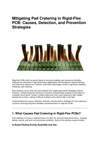
Mitigating Pad Cratering in Rigid-Flex PCB: Causes, Detection, and Prevention Strategies Rigid-flex PCBs offer the perfect blend of structural stability and mechanical flexibility, making them essential in high-performance applications like aerospace, medical devices, and automotive electronics. However, with these advantages comes a significant reliability challenge: pad cratering. Pad cratering occurs when the resin between the copper pad and the fiberglass weave fractures, compromising the electrical connection and potentially leading to intermittent or complete circuit failure. Unlike a simple solder joint crack, pad cratering is often hidden beneath the surface, making it difficult to detect until a device fails in the field. Understanding the causes, detection methods, and prevention strategies for pad cratering is crucial for ensuring long-term durability and performance in rigid-flex PCBs. 1. What Causes Pad Cratering in Rigid-Flex PCBs? Pad cratering is not just a material failure; it's often the result of mechanical stress, improper design choices, and even environmental conditions. Some of the primary causes include: a) Board Flexing During Assembly and Use
Excessive bending or flexing of the PCB—especially near transition points between rigid and flex sections—can put stress on the pad-resin interface, leading to fractures. This is a particular issue in high-reliability applications, where circuit boards may undergo repeated movement, such as wearable medical devices or aerospace control systems. b) Mechanical Shock and Drop Impact Devices that are subject to repeated mechanical shocks, vibrations, or sudden impacts (e.g., automotive control units or military-grade electronics) are more prone to pad cratering. The issue is often exacerbated by large, heavy components that transfer additional stress to solder joints and pads during sudden motion. c) Excessive Force During Testing and Handling In-circuit testing (ICT) and functional testing (FCT) involve test probes that push down on the PCB, potentially flexing it enough to create microscopic fractures. Repeated insertions into card edge connectors or improper handling during assembly can also contribute to stress buildup, eventually leading to pad failure. d) Thermal Expansion and Mismatched CTE (Coefficient of Thermal Expansion) Different materials in a rigid-flex PCB expand at different rates under heat, leading to stress between the pad and the surrounding resin. When a board undergoes repeated temperature cycles (e.g., automotive engine compartments, aerospace electronics), this continuous expansion and contraction weakens the bond over time. 2. How to Detect Pad Cratering? One of the biggest challenges with pad cratering is that it often goes unnoticed until after deployment, when a board fails under real-world stress. Traditional visual inspection techniques cannot reliably identify the issue. Instead, engineers use specialized failure analysis methods: a) Cross-Sectional Microscopy and SEM (Scanning Electron Microscopy) Destructive testing involves cutting the PCB and analyzing the fracture surfaces under a microscope. Scanning Electron Microscopy (SEM) provides detailed imaging of the fractured resin, revealing whether pad cratering occurred. b) Acoustic Microscopy (C-SAM) This non-destructive testing method uses ultrasound waves to detect hidden fractures within the PCB layers.
Frequently used for high-reliability applications, such as aerospace electronics, where early failure detection is critical. c) Electrical Testing and Intermittent Failure Analysis Intermittent failures (connections that work and then fail under mechanical stress) can indicate pad cratering. Techniques like event detectors and real-time monitoring under stress conditions help identify issues before complete failure occurs. d) Dye and Pry Testing This method involves introducing a colored dye into the board and then physically prying components off to see if dye has infiltrated fractures. Useful for quick validation but not always suitable for production-scale analysis. 3. Prevention Strategies: Designing Rigid-Flex PCBs to Minimize Pad Cratering While pad cratering is difficult to eliminate entirely, proper design choices and material selection can significantly reduce its occurrence. Here’s how: a) Choosing the Right Laminate and Stack-Up Configuration High-quality polyimide-based flex materials reduce stress transfer between rigid and flex sections. Using adhesiveless laminates minimizes weak interfaces that could contribute to fractures. Proper layer stack-up design ensures that flex areas transition smoothly into rigid sections, preventing localized stress buildup. b) Optimizing Pad and Via Design Use larger pad diameters and teardrop-shaped pad connections to distribute stress more evenly. Avoid placing vias too close to solder pads, as this weakens the surrounding resin and increases the risk of cratering. Add fillets at flex-to-rigid transitions to reduce localized mechanical stress. c) Minimizing Mechanical Stress During Assembly Reduce in-circuit testing (ICT) probe pressure by using optimized test fixture designs that distribute force more evenly across the board. Avoid pressing on the board during manual handling, especially near high-risk areas like BGA (Ball Grid Array) components. d) Enhancing Solder Joint and PCB Support Use underfill materials on large or heavy components to help absorb mechanical stress.
Opt for low-CTE solder pastes that expand and contract at rates similar to the PCB material, reducing thermal stress. e) Conducting Preemptive Reliability Testing Simulate mechanical stress conditions using finite element analysis (FEA) during the design phase. Perform accelerated life testing (ALT) to identify weak points before production. 4. Conclusion: Engineering Rigid-Flex PCBs for Maximum Durability Pad cratering is a serious but manageable issue in Rigid-Flex PCB, particularly for applications requiring high reliability and mechanical resilience. By understanding the causes, implementing rigorous detection methods, and designing for durability, engineers can significantly improve PCB longevity and reduce field failures. With the right material selection, optimized pad design, and controlled assembly processes, rigid-flex PCBs can withstand even the most demanding environments—from high-speed fighter jets to life-saving medical devices.