Download
1 / 51
640 likes | 1.32k Views
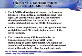
Chapter VIII. Sideband Systems VESTIGIAL SIDEBAND.

E N D
Chapter VIII. Sideband Systems VESTIGIAL SIDEBAND • The 4.2-MHz video signal of commercial broadcast television is transmitted as vestigial sideband (VSB) signal. As illustrated in Figure 8-1, the baseband video signal modulates the carrier in a regular double-sideband/full-carrier (DSB-FC) modulator. • Before power amplification, this AM signal enters the vestigial sideband filter that eliminates most of the lower sideband. • The reason for using VSB is to minimize the transmission spectrum (bandwidth) while maintaining an easily demodulated AM signal; the demodulated low-frequency response of the recovered signal will alsobe better than for single sideband.
Chapter VIII. Sideband Systems VESTIGIAL SIDEBAND Figure 8-1. Generation of vestigial sideband (VSB).
Chapter VIII. Sideband Systems VESTIGIAL SIDEBAND • As seen in Figure 8-2, both sidebands of video signals below 0.75 MHz are transmitted, but only one sideband of the video signals above 0.75MHz is transmitted. • The low frequency video power will be twice that of the high-frequency signals. • If no compensation is provided, the low frequencies will be overemphasized in the picture, and the fine details will be of relatively low contrast (washed out). • This form of frequency distortion is compensated for in TV receiver IF amplifiers.
Chapter VIII. Sideband Systems VESTIGIAL SIDEBAND • Vestigial sideband compensation is accomplished before the demodulation process by providing IF filtering as illustrated in Figure 8-3. • The frequency response of the IF amplifier is designed to roll off linearly between 0.75 MHz of the carrier so that the high video frequencies are emphasized in the IF. • The demodulated video will come out with the same relative amplitudes as it had at the studio.
Chapter VIII. Sideband Systems VESTIGIAL SIDEBAND Figure 8-2. Television video spectrum.
Chapter VIII. Sideband Systems VESTIGIAL SIDEBAND Figure 8-3. VSB compensation filter response.
Double-Sideband/Suppressed-Carrier • The amplitude-modulation technique called double-sideband/suppressed-carrier (DSB-SC) has an important advantage over regular AM (DSB-FC): The carrier is suppressed during the modulation process. • As a result, most of the power in a regular AM transmission, which provides no information, is eliminated.
Double-Sideband/Suppressed-Carrier • EXAMPLE 8-1 : Determine the power savings when the, carrier is suppressed in a regular AM signal modulated to an index of 100%. • Solution: Pt = (1+ m2/2)Pc, Psb = Pc.m2/2. The power savings is (Pt - Psb)/Pt = 1/(1+m2/2) = 1/1.5 = 66.7% for DSB-SC transmission.
Double-Sideband/Suppressed-Carrier • The power savings of Example 8-1 has its price, however. As will be obvious by simple inspection of the waveform of a DSB-SC signal, an AM rectifier cannot be used to demodulate DSB-SC. • Demodulation can be achieved only if a locally generated carrier signal is introduced. • It must not only have exactly the correct frequency (be frequency-coherent) but also have a phase very close to what the carrier would have if it had been transmitted; • that is, DSB-SC demodulation must also be approximately phase-coherent.
Double-Sideband/Suppressed-Carrier • The peak detector discussed for demodulation of regular AM (DSB-FC) will not yield the correct result for DSB-SC. • For instance, when the input is the sinusoidal tone-modulated DSB-SC signal, the output of a peak detector will be the "cusp" signal of Figure 8-10. Fig. 8-10. Result of noncoherent demodulation of DSB-SC.
BALANCED MODULATOR • The circuit used for producing a double-sideband/suppressed-carrier type AM signal is shown in Figure 8-4. • This circuit is a double-balanced mixer in which the diode pair's D1-D2 and D3-D4 are alternately switched on and off by the high-frequency carrier signal vc(t). • The carrier signal could be a sinusoid or squarewave at frequency fc; either way, its amplitude is much larger than that of the information (modulation) signal m(t).
BALANCED MODULATOR Figure 8-4. Balanced ring modulator.
BALANCED MODULATOR • Figure 8-5 shows how the carrier causes alternate reversals, of the polarity of the modulation input signal. • In part A the carrier is positive and diodes D1 and D2 become low-impedance devices for one-half of the RF cycle, while D3 and D4 are essentially open-circuited by reverse bias. • In part B the modulation signal is coupled to the output with reverse polarity because the carrier signal has switched D3 and D4 "on" while reverse-biasing D1 and D2. • The output signal vo(t) is merely m(t) alternately multiplied by +1 and -1 due to the carrier's switching of the diodes. • It should be recognized that due to the balanced output circuit, the carrier signal ideally is not coupled to the secondary of T2.
BALANCED MODULATOR Figure 8-5. Balanced modulator Phase reversals.
BALANCED MODULATOR • The balance is confirmed by following current from a positive polarity vc(t) into the center tap of T1, then splitting and flowing through both. D1 and D2, converging at the center tap of T2 and returning to the vc(t) source. • The opposite flowing currents in the primary of T2 induce voltages of equal magnitude and opposite polarity in the T2 secondary, which therefore cancel each other.
BALANCED MODULATOR • The squarewave switching function can be written with an amplitude of A=p/2 as vc(t) = sin2pfct +(1/3)sin2p(3fc)t +… +(1/n)sin2p(nfc)t (8-1)where n and all previous harmonics are odd only. • The circuit physically performs a function that is mathematically equivalent to multiplication of time-varying signals vc(t) and the information signal m(t). • Hence, the output ism(t) xvc(t) = vo(t) = m(t).sin2pfct + (1/3)m(t).sin2p(3fc)t + higher odd harmonics (8-2)
BALANCED MODULATOR • To illustrate that Equ. (8-2) indeed represents a DSB-SC signal, let the modulation signal be a 2-Vpk audio tone of frequency fm = 5kHz so that m(t) = Asin2pfmt = 2sin2p(5kHz)t V. • Also, let the carrier frequency be fc = 45 kHz. Substituting into Equ. (8-2) yields a modulated output signal of vo(t) = A.sin2pfmt.sin2pfct + (A/3).sin2pfm.sin2p(3fc)t+… = 2.sin2p(5kHz)t.sin2p(45kHz)t + (2/3).sin2p(5kHz)t.sin2p(135kHz)t +…
BALANCED MODULATOR • By the use of the trigonometric identity sinA.sinB = (1/2)[cos(A-B) - cos(A+B)], vo(t)is seen to be vo(t) = (A/2)cos2p(fc-fm)t – (A/2)cos2p(fc+fm)t +(A/6)cos2p(3fc-fm)t – (A/6)cos2p(3fc+fm)t +…(8-3) = cos2p(40kHz)t – cos2p(50kHz)t +(1/3)cos2p(130kHz)t – (1/3)cos2p(140kHz)t +… (8-4)
BALANCED MODULATOR • Figure 8-6 shows a sketch of Equ. (8-4) in both time and frequency domains. • If vo(t) is filtered so that only the first set of sidebands are transmitted, then the harmonics are missing and the result is shown in Figure 8-7. Figure 8-6. Wideband DSB-SC signal.
BALANCED MODULATOR Figure 8-7. DSB-SC after filtering higher harmonics.
Phase Distortion in the Demodulation of Suppressed-Carrier Systems • Figure 8-11 shows the transmitted DSB-SC phasors (a), and the correct relationship between the reinserted carrier and sidebands (b). A phase error Df will result in the AM phasor signal of (c). • The resultant signal in c is a combination of AM and phase modulation, and the demodulated information which might be that of Figure 8-12a would come out like 8 -12b with severe phase distortion.
Phase Distortion in the Demodulation of Suppressed-Carrier Systems Figure 8-11. Phasor representation of DSB-SC. (a) DSB-SC. (b) DSB-SC with carrier “reinserted”-AM. (c) Carrier reinserted with wrong phase. Figure 8-12. Result of phase distortion due to reinserted-carrier phase error. (a) Transmitted. (b) shows the result of a phase distortion due to phase error of reinserted carrier.
Phase Distortion in the Demodulation of Suppressed-Carrier Systems • The demodulated signal has the correct fundamental frequency, but the phase distortion has greatly altered the information. • The phase distortion problem is worse in DSB-SC than in SSB-SC because of the complication introduced by having the two sidebands. • Also, transmission-channel phase shifts, which are not linear between the upper and lower sidebands (envelope-delay distortion), will make the problem even worse.
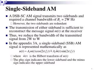
Single-Sideband/Suppressed-Carrier • Single-sideband/suppressed-carrier (SSB-SC) is an amplitude modulations technique used for its outstanding power and bandwidth efficiency. • By eliminating the carrier and one sideband, a power savings of over 83% is realized. Additionally, the band-width required for SSB-SC is theoretically one-half that required when both sidebands are transmitted. • As is the case for DSB-SC, the advantages are somewhat offset by the need for carrier recovery and reinsertion at the receiver. • The phase and frequency accuracy requirements are not as critical for single-sideband as they are for DSB-SC.
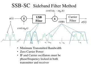
The Sideband-Filter Method • Figure 8-13 shows a block diagram for an SSB-SC transmitter. The heart of this system is the balanced modulator and sideband filter. The information to be communicated is amplified and fed to the balanced modulator. • Also fed to the modulator is an intermediate-frequency (IF) carrier that is frequency- and phase- locked to a stable reference generator in the frequency synthesizer.
The Sideband-Filter Method Figure 8-13. Single-sideband transmitter block diagram (sideband-filter method). Either upper or lower sideband Filtering may be chosen.
The Sideband-Filter Method • The DSB-SC output of the balanced modulator is fed to a sideband filter where the unwanted sideband is eliminated. • The single remaining sideband is at an intermediate frequency and must be up-converted in a mixer to the desired transmission frequency. • After filtering the mixer signal products, the SSB-SC signal is amplified in linear power amplifiers (LPAs) and coupled to the antenna or perhaps to coaxial transmission lines for multiplexing with other single-sideband signals.
The Phase Method of SSB-SC Generation • By properly combining two DSB-SC signals in which either the upper or the lower sidebands are exactly out of phase, a single-sideband signal can be produced. • The equal-frequency sidebands which are out-of-phase will cancel, and the in-phase sidebands reinforce each other to become the transmitted sideband. The block diagram is shown in Figure 8-14.
The Phase Method of SSB-SC Generation Fig. 8-14. SSB transmitter block diagram (phase method).
The Phase Method of SSB-SC Generation • The inputs to the top balanced modulator are sin(wmt) and sin(wct). • The multiplied output is sin(wmt).sin(wct), which by trigonometric identity is sin(wmt).sin(wct) = (1/2)[cos(wc-wm)t - cos(wc+wm)t] (8-5) • The inputs to the bottom balanced modulator are cos(wmt) and cos(wct). • The output of this modulator is cos(wmt).cos(wct) = (1/2)[cos(wc-wm)t + cos(wc+wm)t] (8-6)
The Phase Method of SSB-SC Generation • Equation (8-5) describes DSB-SC with the upper sideband having opposite polarity to the upper sideband of Equ. (8-6). • The output of the summing network is the addition of Eqs. (8-5) and (8-6); that is, SSB-SC output = Vo(t)= (1/2)[cos(wc-wm)t - cos(wc+wm)t] + (1/2)[cos(wc-wm)t + cos(wc+wm)t] = cos(wc - wm)t. (8-7) • The various time waveforms and corresponding frequency spectra for single-tone modulation are shown in Figure 8-15.
The Phase Method of SSB-SC Generation Figure 8-15. Time and frequency spectra for phase method of producing SSB-SC.
The Phase Method of SSB-SC Generation • With integrated circuitry, keeping the phases of modulator inputs and outputs constant when temperatures and power supply voltages are changing is not so simple. • Furthermore, while the carrier phase-shift network at a single frequency is simple enough, the wideband audio network is required to shift the phase by exactly 90° over the full audio frequency range. • The circuit used for this has traditionally been the all-pass network, which is implemented with RC branches (Fig. 8-16). • The desired bandwidth of this network is set between w2 - w1, where w2 = 1/R2C2 is the high-frequency cutoff and w1 is set by the other RC time constant.
The Phase Method of SSB-SC Generation Figure 8-16. Wideband 90° phase-shift circuit.
The Phase Method of SSB-SC Generation • EXAMPLE 8-2: Determine the minimum frequency stability required if a 27.065-MHz oscillator is used to demodulate an SSB-SC voice transmission on Citizen's Band (CB) channel 9. Give the answer in percent and parts per million (ppm). • Solution: The demodulated voice signal will be barely intelligible if the oscillator drifts by 50 Hz. This is 50Hz/27.065 MHz = 1.85 ppm (or 1.85 x 10-6) x 100% = 0.000185%. • On a short-term basis this is achievable with a crystal oscillator. However, one should be concerned about oscillator and received-signal noise.
The Phase Method of SSB-SC Generation • Receivers for SSB-SC are usually a double-conversion type; that is, there are two mixers and two IF systems. • Also, to achieve the frequency stability required when multichannel operation is employed, the LOs and BFO are synchronized to a highly stable reference oscillator.
Frequency Division Multiplexing (FDM) Figure 8.2-1. Typical FDM transmitter. (a) Input spectra and block diagram; (b) baseband FDM spectrum.
Frequency Division Multiplexing (FDM) Figure 8.2-2. Typical FDM receiver.
Frequency Division Multiplexing (FDM) Figure 8-18. Analog telephone FDM hieracrchy.
Frequency Division Multiplexing (FDM) Figure 8-19. Analog telephone FDM frequency spectrum.
QUADRATURE MULTIPLEXING • Quadrature multiplexing is illustrated in Figure 8-20. The two modulation signals m1(t) and m2(t) modulate the quadrature carriers sinwct and coswct in balanced modulators. • The modulated signals are filtered (not shown) to eliminate nonlinear mixer products then linearly added to form the quadrature-multiplexed (QM) signal.
QUADRATURE MULTIPLEXING Figure 8-20. Quadrature multiplexing of two channels. The output is the sum of two orthogonal DSB-SC signals on the same carrier.
QUADRATURE MULTIPLEXING • The QM signal is merely the sum of two orthogonal (90°) DSB -SC signals with the same suppressed-carrier frequency. • To illustrate the principle for a color television application, the color information is transmitted as a vector determined by the amplitude and polarity of the quadrature carriers operating at a frequency of approximately 3.58 MHz relative to the, video carrier. • If, for example, the in-phase carrier has an amplitude of -0.44Vi, where Viis the maximum in-phase carrier voltage of positive polarity, and the quadrature carrier has an amplitude of -0.9Vq, then the TV demodulator should interpret the resulting color as green.
QUADRATURE MULTIPLEXING Figure 8-21. Quadrature multiplexing receiver. The two information signals are m1(t)and m2(t).
QUADRATURE MULTIPLEXING • The receiver LO or beat frequency oscillator (BFO) is synchronized to the incoming signal; that is, the oscillator frequency is exactly wc. • The LO signal 2cos(wct) is split and phase-shifted to quadrature LO signals VLOi = 2cos(wct) and VLOq = 2sin(wct), which are the LO inputs to the in-phase and quadrature mixers, respectively. • The mixer outputs are simply the products of their two input signals -- the received QM signal and the individual LOs.
QUADRATURE MULTIPLEXING • The quadrature mixer output isVLOq x VQM = (2sinwct)[m1(t)sinwct + m2(t)coswct] (8 -8a) =2m1(t)sinwct.sinwct + 2m2(t)sinwct.coswct(8-8b) = m1(t)cos(wc - wc)t - m1(t)cos(wc + wc)t + m2(t)sin(wc - wc)t + m2(t)sin(wc + wc)t(8-8c) = m1(t) - m1(t)cos2wct + m2(t)sin2wct(8-9) • Note that the mixer output is the m1(t) information signal and two 2nd-harmonic mixer products (both DSB-SC), which are easily filtered out with a low-pass filter set just below wc. • Since the low-pass filters (LPF) of Fig. 8-21 have a cutoff frequency of just below wc, the output signal from the "quadrature" branch is VQ(t) = m1(t) (8-10) • A similar analysis shows that VI(t) = m2(t).
Costas Loop for Suppressed Carrier Demodulation • When a pilot signal is transmitted (as is the case for telephone FDM, color TV and FM stereo) a simple phase-1ocked loop will lock onto the pilot for "synchronization.“ • Unfortunately, a suppressed-carrier signal with no pilot has no fixed spectral component on which to lock-up a phase-locked loop. • The sidebands contain information leading to the whereabouts of the missing carrier. • Figure 8-22 shows the additional circuit necessary to extract the required information. • It is a dc-coupled product detector (mixer) known as a phase detector.
Costas Loop for Suppressed Carrier Demodulation Figure 8-22. Costas loop includes BFO-synchronizing for demodulation of all types of suppressed-carrier signals.
Costas Loop for Suppressed Carrier Demodulation • The analysis of the loop for VCO control is as follows: If the VCO (the receiver local oscillator) is locked to the incoming carrier, then wLO = wc and only a small phase error difference (qe) between the two signals will exist. • Because of the small phase error, Equ. 8-8c becomes VLO x VQM = m1(t).cos[(wc-wc)t + qe] - m1(t).cos[(wc+wc)t + qe] + m2(t).sin[(wc-wc)t + qe] + m2(t).sin[(wc+wc)t + qe] = m1(t).cosqe - m1(t).cos(2wct + qe) + m2(t).sinqe + m2(t).sin(2wct + qe) (8-11) • and Equ. (8-10) becomes VQ(t) = m1(t).cosqe (8-12a) andVI(t) = m2(t).sinqe (8-12b)