Download
1 / 14
140 likes | 268 Views
The HV Protection Boards For The RICH Detectors Of LHCb. Claudio Arnaboldi, Tito Bellunato, Paola Gobbo, Davide Luigi Perego and Gianluigi Pessina Istituto Nazionale di Fisica Nucleare (INFN) Università degli Studi di Milano Bicocca - Dipartimento di Fisica

E N D
The HV Protection Boards For The RICH Detectors Of LHCb Claudio Arnaboldi, Tito Bellunato, Paola Gobbo, Davide Luigi Perego and Gianluigi Pessina Istituto Nazionale di Fisica Nucleare (INFN) Università degli Studi di Milano Bicocca - Dipartimento di Fisica P.za della Scienza 3, 20126 Milano, Italy On behalf of the LHCb RICH Collaboration
ABSTRACT We present the circuit protection system for the monitoring of the High Voltage bias for the Hybrid Photon Detectors (HPDs), of the Ring Imaging CHerenkov (RICH) detectors of LHCb. The protection system buffers the voltage lines, attenuated by 12800 V/V, in normal operating conditions and limits the output voltage excursion to the ADC monitoring system to a safe range (between +5 V and -2.5 V) in case of discharge. The circuit is designed to be radiation tolerant. The protection system has been fully characterized with radiation and temperature under the whole expected working conditions of LHCb. Results have shown that the developed protection boards are fully adequate for the whole LHCb lifetime.
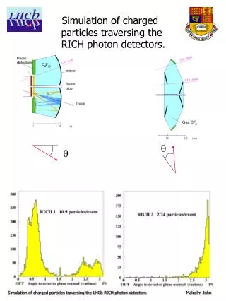
-19.7 KV -20 KV -16.4 KV The detector RICH1 and RICH2 are Ring Imaging CHerenkov detectors at LHCb. Photons generated inside the detector are converted to electrons in 488 Hybrid Photon Detectors (HPD). The HPDs are distributed in columns to form a close-packed configuration: 1/4 of RICH2 Column HPD 100 V Every HPD needs 3 High Voltages, HV, that are responsible of the acceleration, focalization and demagnification of the photo-electrons toward the pixel chip, at about 100 V above GND potential. GND The managing of the HVs is made with PCBs embedded in Silicone rubber.
A A B B C C HV distribution scheme for one column Every column is divided in to 2 half-columns for its HV distribution. A set of boards manages the HV. Every board serves a pair of HPDs. A -20kV A B -19.7kV B C C The -20 KV feeds the Splitter board where the other 2 voltages (-19.7 KV and -16.4 KV) are generated. The Splitter boards also provide biasing to 2 HPDs. The 3 HV's then feed the Intermediate boards that bias a further pair of HPDs, and feed the HVs to the next boards in the chain. The last board of the half-column is the Monitoring board that, as well as biasing a pair of HPDs, generates 3 copies of the HVs attenuated by about 12700 V/V. The attenuated HVs can be readout by the monitoring system. -16.4kV Splitter Intermediate 5G Monitoring One half-column of the RICH
The electrical details of the Monitoring Board The 3 attenuated voltages to be monitored must be protected against any possible discharge. A Surge Arrestor is included on the Monitoring Board to limit to a safe 90 V. This is not enough to prevent permanent damage to the ELMB, the multi-channel ADC system used at LHCb. • Voltage divider(0V , -1.6V) • Surge arrester-90 V We need to add protection We need further protection to be put between the Monitoring board and the ELMB. ELMB safety range -2V - +5V Monitoring lines To ELMB (Embedded LocalMonitor Board)
-19.7 KV -20 KV -16.4 KV Introducing the Protection Board The Protection Board is a buffering system able to copy the voltages to be monitored while assuring the safe condition under any discharge. The specifications the Protection Boards are able to satisfy are: • Unity gain inverting buffering (the ELMB has a larger operating positive range); • Safe margin between -2.5 V and 5 V against 150 V input discharge; • 7 channels per board to manage 6 signals from 2 half-columns and the bias voltage of the Silicon pixel arrays of the same column; • Radiation tolerance against the working location (within the radiation area of LHCb), 9.61011 n/cm2, 700 rad; 5 G 392 K X 2
150 V Protection Board schematic diagram We selected CMOS OAs (Operational Amplifier) having protecting diodes towards the rails at the inputs. 66 K and33 Kresistors have been put in series with the inputs to limit the input current through the diodes to safe limit in case of discharge. 2 unity gain buffer are used to avoid any dropout effect across the seriesresistors, since their negligible input current. Supply voltages are +4.7 V, -4.7 V and -2.1 V. The OAs are biased in such a way the 2 differential output voltages are limited between -2.1 V and 4.7 V under any discharge conditions. The circuit is differential input - differential output with a 15 Hz low pass filter at the output. Accuracy of resistors used was 0.1 %.
Protection Board Characterization A very accurate characterization procedure has been developed. A remote controlled relays system allow to inject signals of known amplitude to simulate discharges. The testing/characterization system was able to manage 5 boards at a time. Characterization was done with temperature (inside an environment chamber) and under irradiation (in a reactor). Discharge -150 V To the Protecting board inputs
Set-up of the characterization system RS-232 Tested parameters against temperature and irradiation: 150 V Power supply Digital driver Environment chamber or Radiation environment • DC Gain; • Linearity • Offset; • Drift; • Discharge; • Voltage Supplies; Switching relays 1 Switching relays 2 PC with MATLAB 5 boards GPIB GPIB Multi-channel multimeter Scope
Discharge simulation Linear regime Repeated input pattern Results example Every characterization test lasted about one day. The input pattern was repeated periodically, every about 1.5 hours. The selected voltage values allowed to fully characterize the channels under test. Output from one channel Discharge The outputs signals were measured in response to the input pattern to study the parameters under investigation. The same set-up was used vs Temperature and Irradiation. Linear regime
Temperature dependance 35 boards with 245 individual channels has been fully tested. No failures have been observed with respect to the simulated discharges. The temperature variation of the gain and the offset has shown that the chosen design and technology is fully compliant with the expected specifications at LHCb. Average result OA outputoffset Gain (0.040±0.730) mV -(0.999±0.002) (0.264±4.640) μV/°C -(0.368±6.280) ppm/°C ΔT(LHCb) ≈ ±5 °C Maximum effect: 0.003 %
Radiation tolerance measurements Irradiation test has been made at the reactor TRIGA MARK II situated in Pavia, IT • The Protection boards will be located in the radiation areaof LHCb where the maximum expected level of radiation after 10 years of data taking is: • γ dose: 700 Rad • Neutron fluence: 9.6 E+111MeV eq ncm-2 We irradiate 3 boards, 6 h each. After this period the level of irradiation applied was: 4·1013 ncm-2 40 x LHCb ~43 kRad 60 x LHCb We gave to the Protection Boards a much larger irradiation dose with respect to that expected during the LHCb lifetime.
Irradiation results The effect of the doses gave a negligible effect. If we limit the irradiation to that expected at LHCb, the red line in the 2 graphs, the effect is even more marginal. Remarks: • it was not possible to find a correlation between the irradiation level and the parameters variations; • The effect of the doses gave a negligible effect - especially if we limit the irradiation to that expected in LHCb, the red line in the 2 graphs. The maximum spread was: Off(1013)– Off(0) = (0.318 ± 0.590) mV G(1013)– G(0) = -(0.071 ± 0.261) %
Conclusions • The monitoring of the HV bias of the HPDs of the RICH1 an RICH2 at LHCb has been performed with a full level of safety; • The protecting circuit that has been designed, built and already in use, has shown outstanding level of accuracy in both the static and dynamic parameters; • Radiation tolerance was found to be more than adequate for the whole lifetime of LHCb.