Download
1 / 13
130 likes | 299 Views
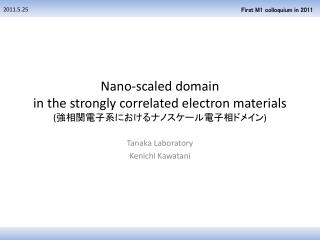
2011.5.25. First M1 colloquium in 2011. Nano -scaled domain in the strongly correlated electron materials ( 強相関電子系におけるナノスケール電子相ドメイン ). Tanaka Laboratory Kenichi Kawatani. Contents. ・ What is the strongly correlated electron system( 強相関電子系 ) ?.

E N D
2011.5.25 First M1 colloquium in 2011 Nano-scaled domainin the strongly correlated electron materials(強相関電子系におけるナノスケール電子相ドメイン) Tanaka Laboratory Kenichi Kawatani
Contents ・What is the strongly correlated electron system(強相関電子系)? ・domain in the strongly correlated electron system ・the merit of picking up domain ・my research
What is the strongly correlated electron system? 3d transiton metal oxides (3d遷移金属酸化物) Organic compounds in the π electron system (π電子系有機化合物) http://www.tuat.ac.jp/ ~naitolab/htsc.html http://www.spring8.or.jp/ja/news_publications /press_release/2009/090320 High temperture superconductor (高温超伝導体) Organic superconductor (有機超伝導体) Various new physical property Recently researched very hardly
The feature of this system 3d orbital restricted π Stimulus Hole-doping Strong Coulomb interaction Electron can’t move easily Decrease of coulomb interaction Electron can move more easily change the physical property drastically
What is domain? water Apparently they are ‘milk’, oil is mixed in the water from micro-scale. oil domain In this system, In this system, ‘domain’ is mixed from micro scale. Insulator metal It maybe caused by ‘ununiformity of electrons’.
Example of observing ‘domain’ Insulator Vanadium dioxide (VO2) ・・・metal-insulator transition M. M. Qazilbash et al. Science 318, 1750 (2007) 1 1 2 2 3 4 3 4 Metal domain Coexistance of insulator and metal phase Whole physical property Average of two phase≠real physical property
Example of picking up the domain Change of physical property by nano-fabrication 10μm 500nm I Yanagisawa et al. Appl. Phys. Lett. 89, 253121 2006 In real, domain change drastically! Change the whole gently Drastic change Picking up the domain Understand the real physical property
Experimental data Research theme・・・the behavior of VO2 metal domain Optical microscope image Metal domain ? I’ll pick up the domain by nano-fabrication, And observe the behavior of VO2 metal domain! I can observe metal domain!
Application for the electronic device Control the metal domain by voltage/current. Multiple-valued memory(多値メモリ) ・・・It can memorize multiple value. Next-generation memory
まとめ In the strongly correlated electron system, ・electrons strongly effect each other ・domainexistance by the ununiformity of electron I will research about the behavior of VO2 metal domain by nano-fabrication. I can get new information about the strongly correlated electron system!
Fabrication method Pulsed laser depositionmethod (PLD法) ~nm Substrate We can make accuracy very thin films (atomic layer).
Nano-fabrication method Nanoimprint lithography method ①making VO2 epitaxial thin film by PLD method ②application of resist by spincoat method ◎TiO2(001)substrate resist VO2 Substrate ③making pattern by nanoimprint equipment ④RIE(Reactive Ion Etching) ⑤remove the resist 100nm~