Experiments by . . .
Solar Cells, Sluggish Capacitance, and a Puzzling Observation Tim Gfroerer Davidson College, Davidson, NC with Mark Wanlass National Renewable Energy Lab, CO ~ Supported by Bechtel Bettis, Inc. and the American Chemical Society – Petroleum Research Fund ~. Experiments by . . .

Experiments by . . .
E N D
Presentation Transcript
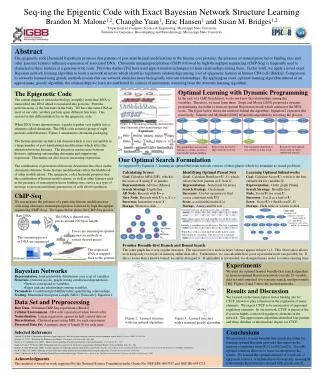
Solar Cells, Sluggish Capacitance, and a Puzzling ObservationTim GfroererDavidson College, Davidson, NCwith Mark WanlassNational Renewable Energy Lab, CO~ Supported by Bechtel Bettis, Inc. and the American Chemical Society – Petroleum Research Fund ~
Experiments by . . . Kiril Simov (Davidson ’05) Patten Priestley (Davidson ’03) and Malu Fairley (Spelman ’03)
Outline • Semiconductors, defects, and solar cells • Diode capacitance and the DLTS experiment • Our measurements and an unusual result • A new model for minority carrier trapping/escape during DLTS
Semiconductors Periodic Potential Physlet
InGaAs Bandgap vs. Alloy Composition Bandgap vs. Lattice Physlet
Semiconductor Defects Lattice-Mismatch Applet Defect Level Physlet (from the forthcoming Physlet Quantum Physics: An Interactive Introduction to Quantum Theory by Mario Belloni et al., due out this Fall
- - - - - + + + + Solar Cell Operation E E - - Field Field Conduction Band ELECTRON ABSORPTION ENERGY CURRENT PHOTON HOLE Valence Band E E - - Field Field When a photon is absorbed, an electron is excited into the conduction band, leaving a hole behind in the valence band. An internal electric field sweeps the electrons and holes away, creating electricity.
- + Defect-Related Trappingand Recombination Conduction Band Defect Level PHONONS ENERGY PHONONS Valence Band But electrons can recombine with holes by hopping through defect levels and releasing phonons (heat). This loss mechanism reduces the efficiency of a solar cell.
- - - + + + Defect-Related Transition Probabilities P ~ 10-1 P ~ (0.5)10 ~ 10-3 P ~ (0.5)16 ~ 10-5 P ~ 10-5 P ~ 10-3 P ~ (0.5)4 ~ 10-1 The probability P of transitions involving phonon emission depends on the number of phonons required, which is determined by the position of the defect level in the gap.
- - - - - - - - - - - - - - + + + + + + + + + + + + + + + + + + + + + + + + + + + + + + + + Depletion Layer p/n Junction Formation P+ N
- - - - - - - - - - + + + + + + + + + + + + + + + + + + + + + + + + + + + + With Bias - - + + Bias-Dependent Depletion P+ N Depletion Layer
Diode Capacitance d1 No bias Vbuilt-in C = DQ/DV ~ e0A/d ENERGY d2 Vbuilt-in+Vapplied Reverse bias Reverse bias increases the separation between the layers where free charge is added or taken away.
- - - - - - - - - - - - + + + + + + + + + + + + + + + + + + + + + + + + + + + + + + + + Depletion Layer With Bias Temporary Reduced Bias Depletion Layer With Bias Temporary Reduced Bias Depletion Layer With Bias - - + + Defect characterization via DLTS P+ N
Computer with LabVIEW (5) Digital Scope(Tektronix) (1) Capacitance meter (Boonton) (2) (4) Oxford 77K Temp Controller (3) Pulse Generator Agilent Cryostat with sample DLTS Experimental Setup
- Conduction Band ENERGY PHOTON + Valence Band Radiative Recombination heat light in light out light in = heat + light out radiative efficiency = light out / light in
ENERGY Defect-Related Density of States Valence Band Conduction Band The distribution of defect levels within the bandgap can be represented by a density of states (DOS) function as shown above.
Radiative Efficiency Measurements light heat
Four Conclusions • 0.29eV hole trap is observed in n-type InGaAs under reverse bias • Temperature-dependent capture and escape rates are symmetrical • Rates level off at cold temperatures due to tunneling • Device modeling points to defect states near the p+/n junction Two References • T.H. Gfroerer et al., APL 80, 4570 (2003). • T.H. Gfroerer et al., IPRM (2005).

