Communication Signals
300 likes | 506 Views
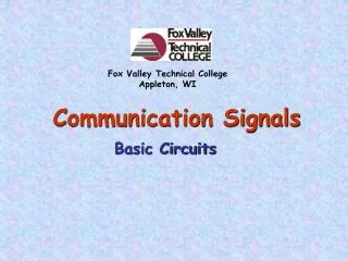
Fox Valley Technical College Appleton, WI. Communication Signals. Basic Circuits. Basic Circuit Parts. Power Supply (e.g. battery) Circuit Protection (e.g. fuse, circuit breaker) Control (e.g. switch) Load (e.g. lamp) Conductors. Pictorial Diagram of A Simple Electric Circuit.

Communication Signals
E N D
Presentation Transcript
Fox Valley Technical College Appleton, WI Communication Signals Basic Circuits G Herlache
Basic Circuit Parts • Power Supply (e.g. battery) • Circuit Protection (e.g. fuse, circuit breaker) • Control (e.g. switch) • Load (e.g. lamp) • Conductors G Herlache
Pictorial Diagram of A Simple Electric Circuit Current Flow Wire Conductor Voltage Source - + Lamps Battery G Herlache
A Schematic Diagram for the Simple Circuit Battery Or DC Voltage Supply PL2 VS PL1 Lamps G Herlache
Hardware Pictorial and Schematic of a Closed CircuitUsing a SPST switch for control Off On Closed Switch - + V I - + Closed Circuit Path => Current Flow G Herlache
Hardware Pictorial and Schematic of an Open CircuitUsing a SPST switch for control Off On Open Switch - + V - + Open Circuit Path => NO Current Flow G Herlache
Example: Pictorial of a SPDT switch controlling two lamps 1 Lamp 1 2 + Switch - Lamp 2 G Herlache
Example: Schematic of a SPDT switch controlling two lamps 1 1 SW SW Lamp 1 Lamp 1 2 2 - + - + V V Lamp 2 Lamp 2 G Herlache
Switch Symbols NCPB NOPB SPST-NC SPDT Break-Make PB SPST-NO Single-pole rotary (6-position) DPST DPDT G Herlache
Typical Mechanical Switches G Herlache
Construction View of a Typical Toggle Switch G Herlache
Chassis Ground DC Ground AC Ground Symbols for Ground G Herlache
A Simple Circuit Schematic Using Ground Symbols I - + 12 V 0 V Ground Symbol G Herlache
V A Ω T Schematic Symbols Introduced So Far Circuit Breaker Fuse Grounds Rheostat Potentio- meter Battery Resistor Lamps SPST-NO SPST-NC NOPB NCPB SPDT Break-Make PB DPST Ammeter Voltmeter Ohmmeter Photo Resistor Thermistor DPDT Rotary Switch G Herlache
Series Circuit IS + V3 − +V1− +V2− IS VS + V4 − +V6− +V5− IS • One path for current. So all components have the same current through them. • But components have different voltages consistent with the voltage – current relationship for each type of component. G Herlache
Parallel Circuit I1 I2 I3 I4 I5 + VS − + VS − + VS − + VS − + VS − VS • One voltage source. So all components have the same voltage across them. • But the components have different currents consistent with the voltage – current relationship for each type of component. G Herlache
Series-Parallel Circuit VS Most circuits are a combination of series and parallel circuits. G Herlache
A node is a connection of a number of circuit components. • A complete node includes all components connected • together electrically Complete Node Partial Node Partial Node Circuit “Nodes” G Herlache
Specialized Electronics Training Basic Logic Circuits G Herlache
Basic Logic Circuits High = +VS = Logic 1 = True = On +VS High ? We don’t know Low = +0 Volts = Logic 0 = False = Off ? Low 0 • Different logic circuit families have different limits for: • Minimum voltage that can be called “high” • Maximum voltage that can be called “low” • There are different names that mean the same thing. G Herlache
Basic Logic Circuits +12V +12V VOut Next Circuit Normally Low (Logic 0) When the switch is open VOut is __?__ volts. When the switch is closed, VOut is __?__ volts. Add a subsequent circuit that supplies a little current through the resistor when the switch is open, and what happens to VOut? G Herlache
Lab Activity Logic with a Normally Open (NO) Switch +12V SW1 10KΩ VOut V 1KΩ Build the circuit initially without the 10KΩ resistor. What is VOut when SW1 is closed? _______________ What is VOut when SW1 is open? _______________ Add the 10KΩ resistor in parallel with SW1. Now what is VOut when SW1 is open? _____________ G Herlache
Basic Logic Circuits +12V +12V • Notice: • The switch is now a normally • closed. • The position of the resistor and • switch are reversed • Therefore: the normal state is still Low. VOut Next Circuit Normally Low (Logic 0) When the switch is open VOut is __?__ volts. When the switch is closed, VOut is __?__ volts. Add a subsequent circuit that absorbs a little current through the resistor when the switch is open, and what happens to VOut? G Herlache
Lab Activity Logic with a Normally Closed (NC) Switch +12V 1KΩ VOut V SW1 10KΩ Build the circuit initially without the 10KΩ resistor. What is VOut when SW1 is closed? _______________ What is VOut when SW1 is open? _______________ Add the 10KΩ resistor in parallel with SW1. Now what is VOut when SW1 is open? _____________ G Herlache
Lab Activity: N.O. Switch Logic(optional) SW1 SW2 SW2 SW1 VOut VOut 9VDC 9VDC R1 470Ω R1 470Ω D1 D1 AND Logic OR Logic G Herlache
Lab Activity: N.C. Switch Logic(optional) • NOTICE: • Series switchesare OR logic now! • Parallel switchesare AND logic now! 470Ω R1 470Ω VOut 9VDC 9VDC R1 D1 SW1 VOut SW2 SW1 D1 SW2 OR Logic AND Logic G Herlache
Logic with N.O. Push Buttons Normally High (Logic 1) Normally Low (Logic 0) AND Logic OR Logic +VS Closed 0V Open +V Closed +V Open 0V COM G Herlache
Logic with N.C. Push Buttons Normally Low (Logic 0) Normally High (Logic 1) OR Logic AND Logic +VS Closed 0V Open +V Closed +V Open 0V COM Notice the change here! G Herlache
Do not use these as logic circuits!!! • This circuit has four • output states: • Both switches open: • V1unconnected • V2unconnected • SW1 closed, SW2 open: • V1 = VS • V2unconnected • SW1 open, SW2 closed • V1unconnected • V2 = 0 Volts • Both switches closed • V1 = VS • V2 = 0 Volts This circuit has the same four output states: SW1 SW1 V1 V1 V2 V2 SW2 SW2 Unconnected outputs have unknown states.. These are not acceptable logic circuits! G Herlache