Band Engineering in MQWs with GQWs for Enhanced LED Performance
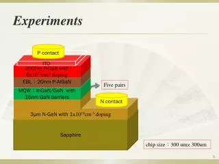
This study explores the impact of band engineering through five pairs of InGaN/GaN multiple quantum wells (MQWs) with quantum dots (GQWs) and conventional quantum wells (QWs) in p-GaN structures with 200 nm thickness and a doping concentration of 6 x 10^17 cm^-3. The epitaxial layers were grown on a sapphire substrate of 300 μm x 300 μm size, featuring n-GaN layers with a doping level of 1 x 10^19 cm^-3. Results include detailed HR-XRD analyses, comparing conventional LEDs to GQW LEDs with varying indium compositions.

Band Engineering in MQWs with GQWs for Enhanced LED Performance
E N D
Presentation Transcript
Experiments P contact ITO 200nm P-GaN with 6x1017cm-3 doping EBL:20nm P-AlGaN Five pairs MQW:InGaN/GaN with 16nm GaN barriers N contact 3μm N-GaNwith 1x1019cm-3 doping Sapphire chip size:300 um× 300um 3
Results and Discussion Fig. 1.Schematic diagram of band engineering at MQWs with GQWs and conventional QWs. 4
Fig. 2. Experimental and simulation HR-XRD curves of (a) conventional LED and (b) GQW LED withindium composition grades from 30% to 0%. 5