Download
1 / 12
120 likes | 140 Views
This feasibility analysis explores the control capabilities of ATMega328 with 18 I/Os and the use of servos in a chassis IO board. It includes calculations for power requirements and protection measures.

E N D
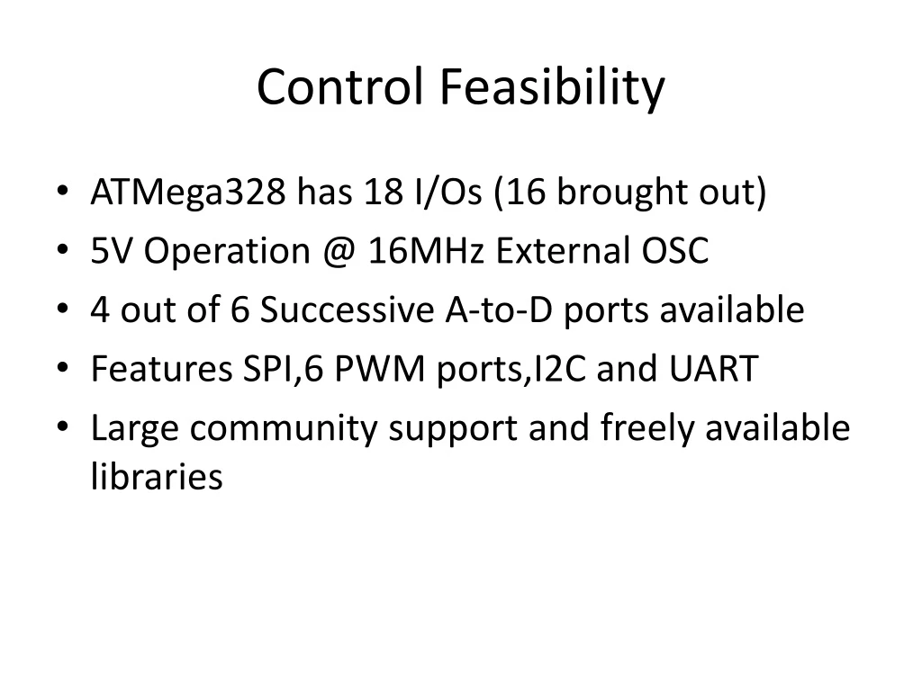
Control Feasibility • ATMega328 has 18 I/Os (16 brought out) • 5V Operation @ 16MHz External OSC • 4 out of 6 Successive A-to-D ports available • Features SPI,6 PWM ports,I2C and UART • Large community support and freely available libraries
Servo Feasibility • Pulse Width Modulation Control • Pulse width determines angle of servo. • Current Measurements: • 700 mA transients • 500 mA under stable load • 40 mA holding idle • 5 mA idle
Servo Feasibility Cont. • Assuming 7.2V 5AH Battery • 5V servo voltage rail (switching buck) • Discharging at 0.1068C (worst case) would take 46.8164 hours to fully discharge Calculations 5V*(.700A*1.1) = 3.85W (Including 10% loss by Buck) 3.85W = 7.2V * IBatt IBatt = 0.5347 A 0.5347A/5AH = 0.1068 C MAX 5AH/0.1068C = 46.8164 hours to full discharge
Protection • Mainboard uses two separate PTCs • Buck protection 3A Trip Current • Control protection 0.1A Trip Current • Buck circuit also includes over current, under voltage, and thermal protection (built into the IC)
Chassis IO Board • Brings out 10 usable IOs to the outside of the LVE • 4 Have Analog In Capabilities • 4 Have PWM Capabilities • 6 Are General I/O • IO Pins Protected By Custom Shroud