Download
1 / 52
810 likes | 1.36k Views
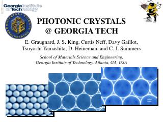
Lecture on Photonic Crystals. 陳啟昌 副教授 國立中央大學 光電科學與工程系. Butterfly crystals. Phys Rev E.67.021907,2003. Spine of sea mouse.

E N D
Lecture on Photonic Crystals 陳啟昌 副教授 國立中央大學 光電科學與工程系
Butterfly crystals Phys Rev E.67.021907,2003
Spine of sea mouse The sea mouse may not look like a mouse, but its hairs are photonic marvels. As the angle of incident light changes, the photonic crystal structure of the spines tunes their reflectance, making new colors appear.
Opal Optics and Photonics News, p.38, Feb, 2003
Famous People Eli Yablonovitch UCLA (Bell Communication Research) Reduction of spontaneous emission Sajeev John University of Toronto (Princeton University) Localization of light
Properties of EM waves 反射(Reflection) 折射(Refraction) 繞射(Diffraction) 干射(Interference) 色散(Dispersion) 極化(Polarization) 波動(wave) 粒子(particle, photon)
Definition of Polarization Plane of incidence Ei Er Br Bi ni Interface qi qr nt Bt qt Et TM TE: transverse electric mode(┴), E perpendicular to PoI TM: transverse magnetic mode(//), E parallel to PoI Brewster’s angle=polarization angle qi+qt=90o r//=0 Application: Test of polarizer
Design of high-reflection coating n1 t1 n2 t2 n1 t1 n2 t2 ns l n0 N pairs Transmission n1t1=l/4 n2t2=l/4 l
1D, 2D and 3D photonic crystals 1D 2D 3D Transmission Photonic bandgap w
Dispersion relation of bulk materials bulk Refractive index of AlxGa1-xN bulk l(nm)=1240/Ephoton(eV)
k and wavelength :Propagation vector k: the magnitude of , propagation number=2p/l
Dispersion relation w=w(k) of waveguide vg2 Slab vg=Dw/Dk n=c/vg vg1 Helmholtz equation:
Band structure of 1D photonic crystal 1D P. C. w p/a -p/a Photonic bandgap k
Reciprocal lattice vector First Brillouin Zone First Brillouin Zone Reciprocal lattice vectors provide a nature basis for optical wavevectors
Ey Ex y Ey x z Band structure of 2D photonic crystal Ex
Electronic band structure and photonic band structure Acta Materialia vol. p.5823, 2003
Crystal Structures Body Centered Cubic Face Centered Cubic Buckyballs C60 Diamond
Diamond, Zinc Blende, FCC, BCC crystal structures ZB Diamond FCC BCC
kz P F L ky D D H G S G N kx First Brillouin zone of 3-D crystal structures kz L L U G Q S ky D S X Z W kx K Body Centered Cubic Face Centered Cubic The centre of the zone, which is characterised by the wave vector , is always denoted by . The points X and L lie at the surface of the first Brillouin zone. It is seen, for example, that the line connecting and X is directed along the crystallographic direction {100} and the line connecting and L is directed along the crystallographic direction {111}.
Scaling law a/l
Defect states Defects Defect states Transmission Defect state Ed Energy
Tools for PBG structure design Finite-Difference Time-domain Method (FDTD) Propagation of electromagnetic field
Tools for PBG structure design Finite-Difference Time-domain Method (FDTD) Mode pattern
Tools for PBG structure design Finite-Difference Time-domain Method (FDTD) Transmission or reflection spectrum
Tools for PBG structure design FDTD method Maxwell equations Yee lattice K. S. Yee, IEEE Trans. Antennas Propagat. Vol. AP-14, p. 302, 1966.
Tools for PBG structure design Plane Wave Expansion Method (PWE) Band structure calculation
Tools for PBG structure design Plane Wave Expansion Method (PWE) Defect mode of photonic crystal structure
Tools for PBG structure design Plane Wave Expansion Method (PWE) Mode patterns
Tools for PBG structure design Multiple Scattering Theory (MST) Data from Prof. Z. Ye Propagation of electromagnetic field
Slab waveguides Effective index neff n1 x Helmholtz equation n2 (1)Finite-difference method n3 (2)Marcatili’s method
neff of SOI structure and cut-off thickness neff nair=1 t nSi=3.46 nSiO2=1.46 t (mm)
Photoresist Spin coating Substrate Patterning Dry Etching Stripper Fabrication techniques e-beam photolithography
E-beam writer in NCU Raith 150 Acceleration voltage: 200-30keV
E-beam photolithography 中央大學光電中心李建階老師提供
Focused Ion Beam Ga source
Collaboration with Dr. M-P Bernal Université de Franche-Comté (France) Using FIB milling PC structure fabricated by FIB in LiNbO3 Period=720nm Radius=200nm 12min , square Period=1mm Radius=300nm 10min , hexagonal
Photonic Crystal Research in NCU FDTD PWE MST E-beam photolithography microspheres PC Waveguides Engineering Theory 葉真 欒丕綱 Design Fabrication 陳啟昌 張正陽 詹益仁 張正陽 李建階 陳暉 綦振瀛 Single photon light source Characterization 陳啟昌 徐子民 張正陽
4吋Si與III-V製程 Equipments Fabrication for 4” Si and III-V
Artificial opal and Inversed opal Nanotechnology 16, 1440, 2005 Applied Surface Science, vol. 217/1-4, pp 281-288, 2003. Desalination, vol. 200, 97, 2006
Output 2 Output 1 Input 1 beamsplitter Input 2 Photonic crystal beam splitters Type II Type I Air holes Dielectric rods Applied Optics, vol.43, p.4188, 2004 US patent: 6,879,432B1, 2004. Optics Communications vol. 259, p.873, 2006
PC directional couplers Conventional waveguides Output port for 1.31mm Output port for 1.55mm PC waveguides Input port Tile 45 degree Top view Optics Express, vol. 13, p.38, 2005.
SHOW-ODR with wafer bonding 1dB/cm (C+L band) for TE and TM modes Large operation bandwidth: C+L band Low propagation loss Low polarization dependent loss Low material dispersion Low non-linearity Low material absorption Micro-fluidic channel Optics Express, vol. 12, p. 6589, 2004. IEEE Photonic Technology Letters, vol.17, 2592, 2005 IEEE J. MEMS 15, 584, 2006
Reflection Coupling between conventional waveguides and PC waveguides Air holes Fabrication in Friedrich Schiller University Jena, Germany PC lens PC taper Opt. Express. Vol. 14, 10759, 2006
GaN photonic crystals ~60nm GaN Appl. Phys. Lett. vol. 89, 071116, 2006 also selected to be published in Virtual Journal of Nanoscale Science & Technology, September 4, 2006 Volume 14, Issue 10
Directional emission from PC waveguides Optics Express vol. 14, 2423, 2006
Transmission spectrum of photonic crystal waveguides with and without microspheres TM TE Optics Express vol. 12, p. 3934, 2004
Partial bandgap or Negative refraction Phys. Rev. B 70, 113101,2004