Download
1 / 31
310 likes | 331 Views
Learn about Mealy and Moore machines, metastability in digital systems, and strategies to minimize its occurrence. Understand the cases and prevention techniques for metastability issues in sequential circuits.

E N D
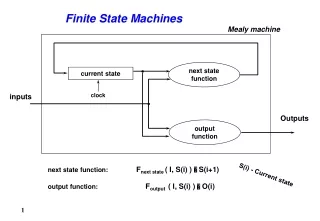
Finite State Machines • Finite State Machines (FSM) are sequential circuit used in many digital systems to control the behavior of systems and dataflow paths. Examples of FSM include control units and sequencers • The state machines are modeled using two basic types of sequential networks- Mealy and Moore. In a Mealy machine, the output depends on both the present (current) state and the present (current) inputs. In Moore machine, the output depends only on the present state.
Mealy FSM • A general model of a Mealy sequential machine consists of a combinatorial network, which generates the outputs and the next state, and a state register which holds the present state as shown below. The state register is normally modeled as D flip-flops. The state register must be sensitive to a clock edge. The other block(s) can be modeled either using the always procedural block or a mixture of the always procedural block and dataflow modeling statements; the always procedural block will have to be sensitive to all inputs being read into the block and must have all output defined for every branch in order to model it as a combinatorial block. • The two blocks Mealy machine fig 1
Moore FSM • A general model of a Moore sequential machine is shown below. Its output is generated from the state register block. The next state is determined using the present (current) input and the present (current) state. Here the state register is also modeled using D flip-flops. Normally Moore machines are described using three blocks, one of which must be a sequential and the other two can be modeled using always blocks or a combination of always and dataflow modeling constructs.
Meta-stability • In General meta-stability is an un-avoidable behavior of the circuit that may cause malfunction. • From a specification point of view, synchronous elements such as flip flops specify a setup time and hold time. • Setup time: data should be stable for this time before arrival of clock • Hold time: data should be hold stable for this time after arrival of clock • Clock calculation depends upon setup time hold time and propagation delay • If setup and hold time is violated then meta-stability will occur.
WHAT IS METASTABILITY? • Meta-stability in digital systems occurs when two asynchronous signals combine in such a way that their resulting output goes to an indeterminate state. A common example is the case of data violating the setup and hold specifications of a latch or a flip-flop. In an ideal world, where all logic designs are synchronous and all inputs are tied to the system clock, meta-stability would not be a concern because all timing conditions for the flip-flops would be met. However, in most of the design, the data is asynchronous w.r.t. the clock making the flop a potential candidate for meta-stability as there’s no reasonable way to insure that the changing asynchronous data will meet the flop’s setup time. Occasionally – not often - the latched data will be corrupt. So the designer has to take care of these violations
WHAT ARE THE CASES, WHEN METASTABILITY OCCURS? • As we have seen that whenever setup and hold violation time occurs, meta-stability occurs, so it is to be seen when does this signal violate this timing requirement. • When the input signal is a asynchronous signal • When the clock skew is more (rise time and fall time is more then the tolerable values). • When interfacing two domains operating at two different frequency. • When the combinational delay is such way that, it changes flip-flop’s input in the required window (setup + hold window)
HOW TO MINIMIZE METASTABILITY? • Synchronize any asynchronous input through one path that has at least one and preferably two flip-flops in series. The flip-flops should be running on the same edge of your system clock as the rest of the circuit. • Design any state machines whose operation is affected by these “synchronized” signals to follow a gray code pattern between states controlled by these signals. Gray Code is a counting scheme where only a single bit changes between numbers • Ensure that setup time of the destination flip-flop is met. This will avoid the creation of metastable conditions inside the circuit and minimize the propagation of any should they occur. • Compute a parity or checksum of the input data before the capture register. Latch that into the register as well. Have the code compute parity and compare it to that read. If there's an error, do another read. • Use metastability hardened Flip-flops.
Noise margin • Noise margin is a parameter closely related to the input-output voltage characteristics. This parameter allows us to determine the allowable noise voltage on the input of gate so that the output will not be affected. • The specification most commonly used to specify noise margin in terms of two parameters. LOW noise Margin NML and High noise Margin NMH
Noise Margin • Note that if either NML or NMH for gate are reduced below 0.1*Vdd, then the gate may be susceptible to switching noise that may be present on the inputs. Apart from considering a single gate , one must consider the net effect of noise sources and noise margins on cascaded gates in assessing the overall noise immunity of a particular system. • Quite often noise margins are compromised to improve speed of the circuit.
Speed Performance • Worst case rise delay= (Rp/n)*(m*n*Cd+Cr+kCg) gate ,drain, routing capacitance, effective resistance of p device in this gate, m-fan-in of gate,k-fanout,n width multiplier of p-device. • Fall delay time = (Rn/n)*(m*n*r*Cg+q(k)*Cg+k*Cg)) • Rp=mRn • BpWp=BnWn/m • *q(k) function of routing capacitance
Clock skew • Clock skew is a phenomenon in synchronous circuits in which the clock signal (sent from the clock circuit or source or clock definition point) arrives at different components at different times.due to • wire-interconnect length • temperature variations • capacitive coupling • material imperfections and • differences in input capacitance on the clock inputs • these factor became more critical for high frequency
Clock Skew-- • Clock skew - Two different flip flop receives the clock signal at slightly different time due to difference in clock net length is called ‘Clock Skew’ but ‘Clock Jitter’ is on same flip flop but position of clock edge moves edge to edge due to some noise in oscillator , power supply variation ot interference by nearby circuitry etc • positive skew • Positive skew occurs when the transmitting register receives the clock tick earlier than the receiving register. • Negative skewNegative skew is occurs when the receiving register gets the clock tick earlier than the sending reg • Zero clock skew refers to the arrival of the clock tick simultaneously at transmitting and receiving reg • Useful Skewclock skew can also benefit a circuit by decreasing the clock period locally at which the circuit will operate correctly, it means skew add more margin to meet setup. that is called useful skew
Clock distribution tree • Need to reduce the skew on distributing the clock • This requires us to reduce the wire delay, and the buffer delay - But we can’t reduce the delay to the required levels (sub 100ps) so • Make the effective delay small, by balancing the delays of all the paths - Change a total delay problem to a matching problem - Make ∆T much smaller than Tdrive Use a clock trees • Match the delay on different branches of tree - If the buffer delay matches - If the wire delay matches - Skew will be zero • Obvious question: - How well can you match delays?
Clock distribution • Clock distribution tree. • H-Tree. • Balance tree network.
Clock Jitter • Jitter is the timing variations of a set of signal edges from their ideal values. Jitters in clock signals are typically caused by noise or other disturbances in the system. Contributing factors include thermal noise, power supply variations, loading conditions, device noise, and interference coupled from nearby circuits.
Types of Jitter • • Period Jitter • • Cycle to Cycle Period Jitter • • Long Term Jitter • • Phase Jitter • • Time Interval Error (TIE)
Period jitter • Period jitter is the deviation in cycle time of a clock signal with respect to the ideal period over a number of randomly selected cycles. If we were given a number of individual clock periods, we can measure each one and calculate the average clock period as well as the standard deviation and the peak-to-peak value. The standard deviation and the peak-to-peak value are frequently referred to as the RMS value and the Pk-Pk period jitter, respectively.
Cycle to Cycle Jitter • Cycle to cycle (C2C) jitter is defined in JEDEC Standard 65B as the variation in cycle time of a signal between adjacent cycles, over a random sample of adjacent cycle pairs. The JEDEC standard further specified that each sample size should be greater than or equal to 1,000. Please note that cycle to cycle jitter only involves the difference in period between 2 consecutive cycles, there is no reference to an ideal cycle.
Long term jitter • Long-term jitter measures the change in a clock’s output from the ideal position, over several consecutive cycles. The actual number of cycles used in the measurement is application dependent. Long-term jitter is different from period jitter and cycle-to-cycle jitter because it represents the cumulative effect of jitter on a continuous stream of clock cycles over a long time interval. That is why long-term jitter is sometimes referred to as the accumulated jitter. Long term jitter is typically useful in graphics/video displays and long-range telemetry applications such as range finders.
Phase jitter • Phase noise is usually described as either a set of noise values at different frequency offsets (e.g., -60 dBc/Hz at 20KHz and -95 dBc/Hz at 10MHz), or as a continuous noise plot over a range of frequencies. Phase jitter is the integration of phase noises over a certain spectrum and expressed in seconds.
Supply and ground bounce • As a module is clocked , the current drawn from the power-supply leads tends to rise as the clock transition. • The current reflects various stages of logic triggered by values changing due to clock transition. • Any gate may change close to clock, large spike may occur. • This is lead to what is termed as “ground bounce” for ground lead and Supply bounce for supply lead. • Ground bounce can also occur in I/O Pads. • Clock buffer can also cause considerable ground bounce in supply leads.
Power distribution Techniques • Power distribution presents several significant problems. • First we must design a global power distribution network that runs both VDD and Vss entirely in metal. • We must size wire properly so that they can handle require current. • We must ensure that the transient behavior of the distribution N/W does not cause a problem for logic to which it supplies current. • Tackle power supply loss (IR loss) • Tackle power supply loss (I*di/dt loss).
Wire Parasitic • Wire Resistance Rlin = *d/z*w (wire resistivity width length hihgt) • Capacitance Side wall, bottom wall, Fringe, plate capacitance. Cline= C.d C capacitance per unit length d length
Signal Integrity Issues • Reflection noise: Due to impedance mismatch, stubs, vias and other discontinuity • Cross talk: Due to electromagetic coupling between signal and vias • Power ground noise: Ground bounce and power bounce • Packaging: Packaging interconnect structure
Signal Integrity Analysis • System specification • Architecture • Interconnect characterization ,I/O Buffer, board and connector • Generate physical design guide lines, noise budget, Timing Budget assessment. • Component placement • Constraint driven layout, final placement, critical routing • Verification ,prototype, lab measurement. • Meets Signal Integrality issues go ached.