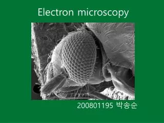
Introduction to Electron Microscopy
Introduction to Electron Microscopy. Fundamental concepts in electron microscopy The construction of transmission and scanning electron microscopes Sample examples of application. Electron Microscope vs. Optical Microscope.

Introduction to Electron Microscopy
E N D
Presentation Transcript
Introduction to Electron Microscopy • Fundamental concepts in electron microscopy • The construction of transmission and scanning electron microscopes • Sample examples of application
Electron Microscope vs. Optical Microscope (first one built in 1931 by Ruska and Knoll) (Leeuwenhoek in 17th century) • Electron vs. Photon Electron: charged, has rest mass, not visible Photon: neutral, has no rest mass, visible at the wavelength ~ 400 nm-760 nm. Because of these differences, the microscope construction will also be different What is the common property?
Comparison of EM and LM a. Similarities (Arrangement and function of components are similar) 1) Illumination system: produces required radiation and directs it onto the specimen. Consists of a source, which emits the radiation, and a condenser lens, which focuses the illuminating beam (allowing variations of intensity to be made) on the specimen. 2) Specimen stage: situated between the illumination and imaging systems. 3) Imaging system: Lenses which together produce the final magnified image of the specimen. Consists of i) an objective lens which focuses the beam after it passes through the specimen and forms an intermediate image of the specimen and ii) the projector lens(es) which magnifies a portion of the intermediate image to form the final image. 4) Image recording system: Converts the radiation into a permanent image (typically on a photographic emulsion) that can be viewed.
Comparison of EM and LM b. Differences1) Optical lenses are generally made of glass with fixed focal lengths whereas magnetic lenses are constructed with ferromagnetic materials and windings of copper wire producing a focal length which can be changed by varying the current through the coil. 2) Magnification in the LM is generally changed by switching between different power objective lenses mounted on a rotating turret above the specimen. It can also be changed if oculars (eyepieces) of different power are used. In the TEM the magnification (focal length) of the objective remains fixed while the focal length of the projector lens is changed to vary magnification. 3) The LM has a small depth of field, thus different focal levels can be seen in the specimen. The large (relative) depth of field in the TEM means that the entire (thin) specimen is in focus simultaneously. 4) Mechanisms of image formation vary (phase and amplitude contrast). 5) TEMs are generally constructed with the radiation source at the top of the instrument: the source is generally situated at the bottom of LMs. 6) TEM is operated at high vacuum (since the mean free path of electrons in air is very small) so most specimens (biological) must be dehydrated (i.e. dead !!). 7) TEM specimens (biological) are rapidly damaged by the electron beam. 8) TEMs can achieve higher magnification and better resolution than LMs. 9) Price tag!!! (100x more than LM)
0.61l/NA Resolution of a microscope Where N.A. is the numerical aperture = n(sina)
The resolution is proportional to the wavelength! Electron equivalent wavelength and accelerating voltage The dualism wave/particle is quantified by the De Broglie equation: λ = h/p = h/mv λ : wavelength; h: Planck constant; p: momentum The energy of accelerate electrons is equal to their kinetic energy: E = eV = m0v2/2 V: acceleration voltage e / m0 / v: charge / rest mass / velocity of the electron These equations can be combined to calculate the wave length of an electron with a certain energy: p = m0v = (2m0eV)1/2 λ = h / (2m0eV)1/2 (≈ 1.22 / V1/2 nm) At the acceleration voltages used in TEM, relativistic effects have to be taken into account (e.g. E>100 keV) λ = h / [2m0eV (1 + eV/2m0/c2)]1/2
Wavelength and accelerating voltage There are other factors that limit the resolution!
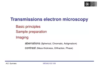
Types of Electron Microscope • Transmission Electron Microscope (TEM) uses a wide beam of electrons passing through a thin sliced specimen to form an image. This microscope is analogous to a standard upright or inverted light microscope • Scanning Electron Microscope (SEM) uses focused beam of electrons scanning over the surface of thick or thin specimens.. Images are produced one spot at a time in a grid-like raster pattern. (will be discussed in a later lecture) • Scanning Transmission Electron Microscope (STEM) uses a focused beam of electrons scanning through a thin sliced specimen to form an image. The STEM looks like a TEM but produces images as does an SEM (one spot at a time). It is most commonly used for elemental analysis of samples.
FEI Tecnai 20 For TEM, since the electrons need to penetrate the specimen, it must be very thin (< 100 nm)
Leo 982 SEM For SEM: a fine probe (beam spot) is formed by condenser lens and its size determines the resolution (this differs from the TEM which is diffraction limited)
Electron Gun FEG W hairpin LaB6 crystal
Thermionic Sources Increasing the filament current will increase the beam current but only to the point of saturation at which point an increase in the filament current will only shorten the life of the emitter
Condenser-lens system C1 controls the spot size The condenser aperture must be centered C2 changes the convergence of the beam
TEM imaging modes Bright field/dark field depends on the aperture position. Modern way for diffraction tilts the beam instead of moving the aperture
STEM image Bright and dark field STEM image of Au particles on a carbon film What is the differences between this dark field and the previous one?
Magnification in TEM Mob × Mint × Mproj = Total Mag Depends on the magnification, some lens may not be used
Backscattered Electrons: Formation Caused by an incident electron colliding with an atom in the specimen which is nearly normal to the incident's path. The incident electron is then scattered "backward" 180 degrees. Utilization The production of backscattered electrons varies directly with the specimen's atomic number. This differing production rates causes higher atomic number elements to appear brighter than lower atomic number elements. This interaction is utilized to differentiate parts of the specimen that have different average atomic number.
Backscatter Detector The most common design is a four quadrant solid state detector that is positioned directly above the specimen
Gold particles on E. coli appear as bright white dots due to the higher percentage of backscattered electrons compared to the low atomic weight elements in the specimen
Secondary Electrons: Source Caused by an incident electron passing "near" an atom in the specimen, near enough to impart some of its energy to a lower energy electron (usually in the K-shell). This causes a slight energy loss and path change in the incident electron and the ionization of the electron in the specimen atom. This ionized electron then leaves the atom with a very small kinetic energy (5eV) and is then termed a "secondary electron". Each incident electron can produce several secondary electrons. Utilization Production of secondary electrons is very topography related. Due to their low energy, 5eV, only secondaries that are very near the surface (< 10 nm) can exit the sample and be examined. Any changes in topography in the sample that are larger than this sampling depth will change the yield of secondaries due to collection efficiencies. Collection of these electrons is aided by using a "collector" in conjunction with the secondary electron detector. The collector is a grid or mesh with a +100V potential applied to it which is placed in front of the detector, attracting the negatively charged secondary electrons to it which then pass through the grid-holes and into the detector to be counted.
A conventional secondary electron detector is positioned off to the side of the specimen. A faraday cage (kept at a positive bias) draws in the low energy secondary electrons. The electrons are then accelerated towards a scintillator which is kept at a very high bias in order to accelerate them into the phosphor.
The position of the secondary electron detector also affects signal collection and shadow. An in-lens detector within the column is more efficient at collecting secondary electrons that are generated close to the final lens (i.e. short working distance).
Secondary Electron Detector Side Mounted In-Lens What are the differences between these two images?
Auger Electrons Source Caused by the de-energization of the specimen atom after a secondary electron is produced. Since a lower (usually K-shell) electron was emitted from the atom during the secondary electron process an inner (lower energy) shell now has a vacancy. A higher energy electron from the same atom can "fall" to a lower energy, filling the vacancy. This creates and energy surplus in the atom which can be corrected by emitting an outer (lower energy) electron: an Auger Electron. Utilization Auger Electrons have a characteristic energy, unique to each element from which it was emitted from. These electrons are collected and sorted according to energy to give compositional information about the specimen. Since Auger Electrons have relatively low energy they are only emitted from the bulk specimen from a depth of < 3 nm
X-rays Source Caused by the de-energization of the specimen atom after a secondary electron is produced. Since a lower (usually K-shell) electron was emitted from the atom during the secondary electron process an inner (lower energy) shell now has a vacancy. A higher energy electron can "fall" into the lower energy shell, filling the vacancy. As the electron "falls" it emits energy, usually X-rays to balance the total energy of the atom so it. Utilization X-rays or Light emitted from the atom will have a characteristic energy which is unique to the element from which it originated. (will be discussed in a separate lecture)
Unscattered Electrons Source Incident electrons which are transmitted through the thin specimen without any interaction occurring inside the specimen. Utilization The transmission of unscattered electrons is inversely proportional to the specimen thickness. Areas of the specimen that are thicker will have fewer transmitted unscattered electrons and so will appear darker, conversely the thinner areas will have more transmitted and thus will appear lighter.
Elasticity Scattered electrons Source Incident electrons that are scattered (deflected from their original path) by atoms in the specimen in an elastic fashion (no loss of energy). These scattered electrons are then transmitted through the remaining portions of the specimen. Utilization All electrons follow Bragg's Law and thus are scattered according to ml=2*d*sin q (angle of scattering). All incident electrons have the same energy(thus wavelength) and enter the specimen normal to its surface. All incidents that are scattered by the same atomic spacing will be scattered by the same angle. These "similar angle" scattered electrons can be collated using magnetic lenses to form a pattern of spots; each spot corresponding to a specific atomic spacing (a plane). This pattern can then yield information about the orientation, atomic arrangements and phases present in the area being examined.
The diffraction pattern is highly dependable on the structure of the specimen Dr. Schroeder will have a lecture dedicated to diffraction
Inelastically Scattered Electrons Source Incident electrons that interact with specimen atoms in a inelastic fashion, loosing energy during the interaction. These electrons are then transmitted trough the rest of the specimen Utilization Inelastically scattered electrons can be utilized two ways Electron Energy Loss Spectroscopy (EELS): The inelastic loss of energy by the incident electrons is characteristic of the elements that were interacted with. These energies are unique to each bonding state of each element and thus can be used to extract both compositional and bonding (i.e. oxidation state) information on the specimen region being examined. Kikuchi Bands: Bands of alternating light and dark lines that are formed by inelastic scattering interactions that are related to atomic spacings in the specimen. These bands can be either measured (their width is inversely proportional to atomic spacing) or "followed" like a roadmap to the "real" elasticity scattered electron pattern.
EELS of NiO Combine with STEM, can do element mapping in TEM: compare to EDX, EELS is better for lighter elements Unlike diffraction pattern blinks on and off, the Kikuchi line pattern rotates when one tilts the crystal. Thus is helpful in orientating a crystal to certain zone axis.
Specimen interaction volume • Atomic number of the material being examined; higher atomic number materials absorb or stop more electrons and so have a smaller interaction volume. • Accelerating voltage being used; higher voltages penetrate farther into the sample and generate larger interaction volumes • Angle of incidence for the electron beam; the greater the angle (further from normal) the smaller the volume
Monte Carlo simulation of the interaction volume Try the online simulation at: http://www.matter.org.uk/tem/electron_scattering.htm
(r) - electron (r) - potential q(r) - exit-wave function sample Fourier transform Objective lens transfer function I(H)=|Q(H)|2 Q(H)T(H) Q(H) atoms Backfocal Plane Inverse Fourier transform I(r)=|(r)|2 I(r) Sample thickness (r) image Plane High-Resolution Electron Microscopy Wave functions for elastically-scattered, forward electrons • For a weak phase object, the observable image intensity is: • I=1 - 2(r) FFT[T(H)]. • represents convolution. This shows a pure phase-contrast image. Illustration of electron wave passing through under phase object approximation. The phase changes (contrast) is imaged.
High resolution Images Discovery of the carbon nanotube Pt nanoparticles S. Iijima, Nature 354, 56 (1991).