Download

1 / 14
150 likes | 392 Views
Kelsey Poineau Research Advisor: Sid Ghosh. Optimization of Passivation for Mid and Long Wavelength InAs/GaSb Superlattice Photodetectors. Infrared Detection. Any object at non-zero temperature emits heat (electromagnetic radiation)

E N D
Kelsey Poineau Research Advisor: Sid Ghosh Optimization of Passivation for Mid and Long Wavelength InAs/GaSb Superlattice Photodetectors
Infrared Detection • Any object at non-zero temperature emits heat (electromagnetic radiation) • Use infrared wavelengths because they have good transmittance through the atmosphere
Motivation • Detection of mid- and long-wavelength infrared radiation is important in many industries • InAs/GaSb type-II superlattice materials have potential to outperform existing detectors • Limited by poor surface quality
How to Detect Infrared Radiation IR Detector Electrical IR Radiation Detector Output Optical Magnetic Object Solid State Material Semiconductor If Eph>EG, photons can be absorbed and create free electrons in conduction band Photogenerated electrons can be used as the detector output
p-i-n detectors • IR photons absorbed in the depletion region generate an electron-hole pair; the electric field sweeps the electron to the n-side and hole to the p-side • Ideally, no current so when an incoming photon creates an electron-hole pair it is detected
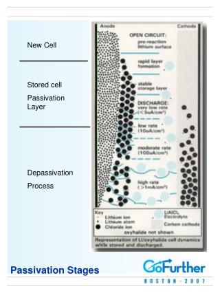
Surface leakage considerably limits LWIR device performance Native Oxides Charged ions Interfacial traps Surface passivation provides a viable solution Passivating layer over semiconductor surfaces prevents current flow in oxide and terminates unsatisfied bonds Problem III-V Semiconductor Wafers
Project Goal • Comparative study of passivants (SiO2,SiN, ZnS) • ZnS degrades over time • Stacked passivation • Investigated to enhance long term stability of interface between passivation layer and InAs/GaSb substrate • ZnS/Silicon nitride • ZnS/Silicon oxide • Compared on basis of electrical properties and device performance
Work to date • Stacked passivation • Unable to achieve good electrical insulation • Considering alternatives: SiN thin films • Advantages • High quality dielectric • Hard and strong • High resistivity • Low porosity • Disadvantages • Effects of surface leakage in SiN>ZnS • Possess high mechanical strain
Laying the groundwork • Strain may increase surface leakage and degrade passivation qualities • Passivate with multiple Si/N ratios to study electrical characteristics • Plasma-enhanced Chemical Vapor Deposition (PECVD) • Vary gas flow rates of silane and ammonia
Low-stress SiN films • Change mechanical properties of SiN films French, J. P., and P. M. Sarro. "Optimization of a low-stress silicon nitride process for surface-micromachining applications." Sensors and Actuators A 58 (1997): 149-57
Preliminary Results • PECVD Parameters • Flow Rates • SiH4 (silane) - 500 sccm • NH3 (ammonia) - 70 sccm • Chamber Pressure - 650 mtorr • Temperature - 300°C • RF power - 20 W • Time - 15 mins • Ellipsometer Data • Thickness - 265 nm • Refractive Index - 1.95
Summary • Analysis of surface states is key to finding and understanding improved processing leading to increased performance in devices • Could not examine effectiveness of stacked passivation in preventing ZnS degradation over time • Expect low stress (silicon-rich) silicon nitride films will improve device performance compared to stiochometric Si3N4 passivation layers
References • French, J. P., and P. M. Sarro. "Optimization of a low-stress silicon nitride process for surface-micromachining applications." Sensors and Actuators A 58 (1997): 149-57. • Pierret, Robert F. Semiconductor Device Fundamentals. N.p.: Addison-Wesley Company, Inc, 1996. Print. • Prineas, J. P., Mikhail Maiorov, and C. Cao. "Processes Limiting the Performance of InAs/GaSb Superlattice Mid-Infrared PIN Mesa Photodiodes." Proceedings of SPIE, the international Society for Optical Engineering 6119 (2006). • Saraswat. "Integrated Circuit Isolation Technologies." Http://www.leb.eei.uni- erlangen.de/winterakademie/2008/courses/course3_material/backEnd /Isolation_notes.pdf. • Streetman, Ben G., and Sanjay Kumar Banerjee. Solid State Electronic Devices. 6th ed. Upper Saddle River, New Jersey: Pearson Prentice Hall, 2006. Print.
Acknowledgements Special thanks to my advisor Professor Sid Ghosh and Koushik Banerjee. This project was funded by the National Science Foundation and the Department of Defense from the EEC-NSF Grant # 0755115. Additional financial support was awarded by the National Science Foundation from the CMMI-NSF Grant # 0925425. Questions?