MURI, year started: 1998
Compact Power Supplies Based on Heterojunction Switching in Wide Band Gap Semiconductors Robert Davis, North Carolina State University email: robert_davis@ncsu.edu http://muriserver.mte.ncsu.edu Contract: ONR MURI N000014-98-1-0654. MURI, year started: 1998. March 2002. Objectives:

MURI, year started: 1998
E N D
Presentation Transcript
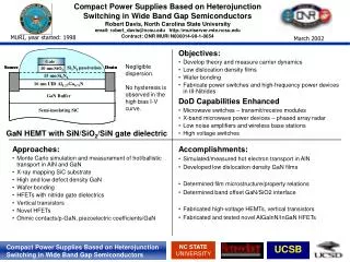
Compact Power Supplies Based on Heterojunction Switching in Wide Band Gap SemiconductorsRobert Davis, North Carolina State Universityemail: robert_davis@ncsu.edu http://muriserver.mte.ncsu.eduContract: ONR MURI N000014-98-1-0654 MURI, year started: 1998 March 2002 Objectives: • Develop theory and measure carrier dynamics • Low dislocation density films • Wafer bonding • Fabricate power switches and high-frequency power devices in III-Nitrides DoD Capabilities Enhanced • Microwave switches – transmit/receive modules • X-band microwave power devices – phased array radar • Low noise amplifiers and wireless base stations • High voltage switches Negligible dispersion.No hysteresis is observed in the high bias I-V curve. GaN HEMT with SiN/SiO2/SiN gate dielectric • Approaches: • Monte Carlo simulation and measurement of hot/ballistic transport in AlN and GaN • X-ray mapping SiC substrate • High and low defect density GaN • Wafer bonding • HFETs with nitride gate dielectrics • Vertical transistors • Novel HFETs • Ohmic contacts/p-GaN, piezoelectric coefficients/GaN • Accomplishments: • Simulated/measured hot electron transport in AlN • Developed low dislocation density GaN films • Determined film microstructure/property relations • Determined band offset GaN/SiO2 interface • Fabricated high-voltage HEMTs, vertical transistors • Fabricated and tested novel AlGaInN/InGaN HFETs