Charge Carrier Related Nonlinearities
130 likes | 394 Views
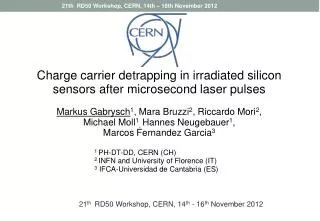
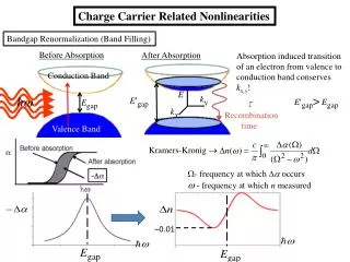
- frequency at which occurs - frequency at which n measured. 0.01. E gap. E gap. Charge Carrier Related Nonlinearities. Bandgap Renormalization (Band Filling). Absorption induced transition of an electron from valence to conduction band conserves k x,y !.

Charge Carrier Related Nonlinearities
E N D
Presentation Transcript
- frequency at which occurs • - frequency at which n measured 0.01 Egap Egap Charge Carrier Related Nonlinearities Bandgap Renormalization (Band Filling) Absorption induced transition of an electron from valence to conduction band conserves kx,y! Conduction Band Valence Band Before Absorption After Absorption Egap Egap>Egap Egap Recombination time Kramers-Kronig ky E kx
Charge Carrier Nonlinearities Near Resonance • Most interesting case is GaAs, carrier lifetimes are nsec effective e (linewidths) meV • classical dispersion (Haug & Koch) is of form . • near resonance, as discussed before • Ee – electronenergy level to which electron excited in conduction band • Eh – electron energy level in valence band from which electron excited by absorption • Simplest case of a 2 band model:
“Transparency point” Gain 0 Loss - - Active Nonlinearities (with Gain) Optical or electrical pumping Stimulated emission Get BOTH an index change AND gain! Kramers-Krönig used to calculate index change n() from (). Ultrafast Nonlinearities Near Transparency Point At the transparency point, the losses are balanced by gain so that carrier generation by absorption is no longer the dominant nonlinear mechanism for index change. Of course one gets the Kerr effect + other psand sub-psphenomena which now dominate.
Evolution of carrier density in time “Spectral Hole Burning” “hole” in conduction band due to to stimulated emission at maximum gain determined by maximum product of the density of occupied states in conduction band and density of unoccupied states in valence band “Carrier Heating” (Temperature Relaxation) electron collisions return carrier distribution to a Fermi distribution at a lower electron temperature SHB – Spectral Hole Burning Experiments have confirmed these calculations!
Semiconductor Response for Photon Energies Below the Bandgap As the photon frequency decreases away from the bandgap, the contribution to the electron population in the conduction band due to absorption decreases rapidly. Thus other mechanisms become important. For photon energies less than the band gap energy, a number of passive ultrafast nonlinear mechanisms contribute to n2 and 2. The theory for the Kerr effect is based on single valence and conduction bands with the electromagnetic field altering the energies of both the electrons and “holes”. There are four processes which contribute, namely the Kerr Effect, the Raman effect (RAM), the Linear Stark Effect (LSE) and the Quadratic (QSE) Stark Effect. Shown schematically below are the three most important ones. The theoretical approach is to calculate first the nonlinear absorption and then to use the Kramers-Kronig Relation to calculate the nonlinear index change . - frequency at which occurs - frequency at which n calculated
Kerr Here Ep (“Kane energy”) and the constant Kare given in terms of the semiconductor’s properties. K=3100 cm GW-1 eV5/2
QSE Kerr
Quantum Confined Semiconductors When the translational degrees of freedom of electrons in both the valence and conduction bands are confined to distances of the order of the exciton Bohr radius aB, the oscillator strength is redistributed, the bandgap increases, the density of states e(E) changes and new bound states appear. As a result the nonlinear optical properties can be enhanced or reduced) in some spectral regions. Quantum Wells -Absorption edge moves to higher energies. -Multiple well-defined absorption peaks due to transitions between confined states -Enhanced absorption spectrum near band edge
Example of Multi-Quantum Well (MQW) Nonlinearities • Nonlinear absorption change (room temp.) • measured versus intensity and converted • to indexchange via Kramers-Kronig Index change per excited electron A factor of 3-4 enhancement!! Quantum Dots Quantum dot effects become important when the crystallite size r0 aB (exciton Bohr radius). For example, the exciton Bohr radius for CdSaB = 3.2nm, CdSeaB = 5.6nm, CdTeaB = 7.4nm and GaAsaB = 12.5nm. Definitive measurements were performed on very well-characterized samples by Banfi. De Giorgio et al. in range aBr0 3aB Measurements at1.2m (), 1.4m () and 1.58m () for CdTe Measurements at 0.79m (+) for CdS0.9Se0.1 Note the trend that Im{(3)} seems to fall when aBr0 !
Nonlinear Refraction and Absorption in Quantum Dots for aBr0 3aB: II-VI Semiconductors Experimental QD test of the previously discussed off-resonance universal F2(x,x) and G2(x,x) functions for bulk semiconductors (discussed previously) by M. Sheik-Bahae, et. al., IEEE J. Quant. Electron. 30, 249 (1994). 2 10-18 0 • Nanocrystals • + 0.79m • 2.2 m • 1.4 m • 1.58m 0.7 0.5 0.6 0.8 10-19 Real{(3)} in units of 10-19m2V-2 -2 (/0)4Imag{(3)} in units of m2V-2 10-20 Bulk CdS 0.69m ▼ CdTe 12, 1.4, 1.58m -4 10-21 2.0 1.5 1.0 To within the experimental uncertainty (factor of 2), no enhancements were found in II-VI semiconductors for the far off-resonance nonlinearities!