Download
1 / 30
300 likes | 314 Views
This report discusses the status of Compton imaging projects using silicon radiation detectors for photon detection and energetic electron detection in medical imaging. It covers the detection of photons and electrons in semiconductor detectors, photon interactions in silicon, attenuation of incoming photons in materials, range of electrons in materials, limitations in imaging modalities with scintillators, and R&D projects using silicon detectors in medical imaging within the CIMA Collaboration.

E N D
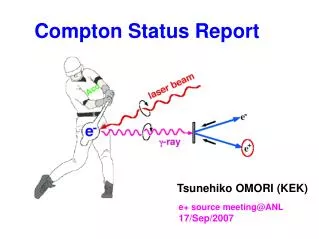
Status Of Compton Imaging Projects Carried Out In The CIMA Collaboration HPD Brain PET Meeting Bari 16. 01. 2007 P. Weilhammer INFN Perugia/CERN Status Report On Compton Imaging Projects
OUTLINE of Presentation 1. Photon Detection with Silicon Detectors (A few trivial notions) 2. Two Projects Involving the Compton Camera Concept Using Silicon Radiation Detectors Status Report On Compton Imaging Projects
Detection of Photons and Energetic Electrons in Semiconductor Detectors • Medical imaging requires good ability of detection of photons, in reality detection of energetic electrons created inside the material ( an advantage!), over a wide range of energies. • Energy Ranges: • Single Photon Emission Tomography (SPECT):detect g-rays for a big variety of isotopes used in different tracer molecules, e.g. • 99mTc 140 keV • 111In185 and 245 keV • 31I 360 keV • Positron Emission Tomography (PET):511 keV g or ~50 keV to 350 keV Compton recoil electrons Status Report On Compton Imaging Projects
Photon Interactions in Silicon Only two out of all photon interactions are important for medical imaging: In traditional imaging applications the “wanted” one: Photoelectric Absorption(total absorption of g or X-ray) s = 4√2 a4Eg-7/2Z5sTh with the Thomson cross-section sTh.= 8p/3 r20 = 6.652 bars per electron. Status Report On Compton Imaging Projects
The “unwanted” one:Compton scattering Kinetic energy of recoil electron q The recoil electron ( from K-shell or L-shell or valence band) creates (eh) pairs in the semiconductor bulk through ionization Status Report On Compton Imaging Projects
Attenuation of incoming photons in material In 1mm thick silicon for 20 keV photons Photoelectric interaction: ~ 97% Compton interactions: ~3% Interesting region for medical imaging Interactions/m for Si versus photon energy Status Report On Compton Imaging Projects
Range of Electrons in Materials The range of electrons in materials expressed as range * density is very similar for many different materials Typical Range of Compton recoils: 50 keV electron in silicon: ~20 mm 200 keV : ~200 mm 500 keV :~ 600 mm For Compton interaction the medical imaging “point-like” domain is between 10 keV and 250 to 300 keV! NaI Range*density [g/cm2] Si 10-2 100 keV Status Report On Compton Imaging Projects
Some inherent physical limitations in different imaging modalities with scintillators are: • Spatial extension of the photon interaction in the detector material due to the nature of photon interactions (in most materials interaction cascades are frequent before final absorption). The typical extension of a photon interaction in many detector materials ( at 500 keV) can be considered to be confined in a sphere of ~1 cm in diameter. • Depth of Interaction Parallax error • Finite path length of positrons and recoil electrons • Compton scattering in tissue. • In PET: Finite momentum of e+e- compound at the moment of decay Acolinearity • Accidental coincidences. • ……… ~1cm through multiple interactions in scintillator Incoming g Status Report On Compton Imaging Projects
An Observation: What about Silicon Radiation Sensors which are NOW part of Scanners or Cameras used in Hospitals Photo-diode arrays in present day X-Ray CT (mostly Hamamatsu ) Low Dose digital Mammography Scanner from SECTRA (single sided strip detectors and VLSI Front-end) See www.sectra.com Autoradiography Camera from BIOMOLEX (double sided strips and VLSI Front-end) See www.biomolex.no And some more……… but it is a niche market except fror photo-diodes Status Report On Compton Imaging Projects
R&D Projects using Silicon Detectors in Medical Imaging within the CIMA Collaboration • Novel axial brain PET Scanner • Compton Camera and Probes • High resolution small animal PET scanner based on Compton interactions Status Report On Compton Imaging Projects
Compton Imaging Status Report On Compton Imaging Projects
The main features of Compton Imaging are: • The Mechanical collimator in the Anger Camera is replaced by “Electronic Collimation”. This removes the coupling between sensitivity and spatial resolution. • This is achieved by having two detectors in coincidence: • In the first detector the gamma rays are scattered by Compton Scattering on electrons in the detector material • In the second detector the scattered gamma ray is absorbed Status Report On Compton Imaging Projects
The measured quantities in Compton imaging are: x, y, z-co-ordinates in the first detector x, y, z-co-ordinates in the second detector Energy of recoil electron in first detector Energy of scattered photon in second detector Not measurablewith Compton Cameras for medical applications: Direction of recoil electron,which leads to the conical ambiguity. This leads to more complicated image reconstruction algorithms. • Expected improvements over Anger Camera: • Factor ~5 in spatial resolution for probes • Factor 5 to 50 improvement in sensitivity Status Report On Compton Imaging Projects
Results from a Demonstrator Test in 2005 Status Report On Compton Imaging Projects
The Silicon Pad Sensors All possible solutions need to be cheap and standard technology readily available in Industry. Modifications to a technology need to be available in the standard industrial processes A processed wafer 1mm thick Schematic cross section of double metal pad sensor 10 cm Routing lines end at external bond pad rows for connection to readout chip Details of routing technology on pads via double metal vias Status Report On Compton Imaging Projects
Silicon detector and stack of 5 detectors Status Report On Compton Imaging Projects
A Demonstrator set-up with stack of 5 Silicon pad sensor and 3 camera heads Status Report On Compton Imaging Projects
Main Results Spatial resolution was measured for 4 energies; 57Co (122 keV) and 133Ba (272,302 and 356 keV). For the highest energy with a source-first detector distance of 11.3 cm: 5mm FWHM With a source Si distance of 3 cm this gives (simulation)2 -3 mm FWHM Status Report On Compton Imaging Projects
Status: Spatial resolution in Silicon Demonstrated Next Demonstrator test foreseen before end of 2006 with much improved camera head and improved silicon ( lower thresholds possible) Status Report On Compton Imaging Projects
A High Resolution Small Animal PET Scanner based onCompton Scatter Eventsin Silicon Pad Detectors Status Report On Compton Imaging Projects
~ 1 cm Resolution Limitations for Conventional PET Inter-Crystal Scattering Depth of Interaction Uncertainty Scintillator • Multiple Interactions • Energy deposited over a volume • ~ 1 cm mean path • Penetration into crystals widens LOR Best Resolution ~ 1.5-2 mm
BGO detector Si detector Si-Si Si-BGO BGO-BGO A Very High Resolution PET Scanner for small animals based on Compton Scattering events is proposed: Three Major Coincidence Events The Concept Si-Si : Very High Resolution Si-BGO : High Resolution BGO-BGO : Conventional PET Resolution Status Report On Compton Imaging Projects
Simulation results with this configuration Efficiency for different event classes BGO ring Calculated for point source in center plane. Only single scattering or absorption interactions in the silicon detector are included. Back scattered photons from BGO and events without full energy deposition are excluded. Status Report On Compton Imaging Projects
Compton PET Test Bench Silicon detector BGO detector VATAGP3 HAMAMATSU PMT R2497 4.5 cm 2.2 cm and 1 mm thick 3216 (512) pads, 1.4 mm 1.4 mm pixel size Energy Resolution 1.39 keV FWHM for Tc 99m 5.3 cm 5 cm and 3 cm thick 84 array, 12.5 mm 5.25 mm crystal size Energy Resolution 22% FWHM for Na-22
Prototype PET Instrument Single-slice instrument using silicon and BGO Silicon detector Silicon detector Disassembled Assembled
Resolution Uniformity 5 4 3 2 1 0 0 1 2 3 4 5 cm Sinogram Source pairs at 5, 10, 15, & 20mm off-axis The sources in each pair are clearly separated at appropriate sinogram angles
5 4 3 2 1 0 0.254 mm 0.127 mm 5 4 3 2 1 0 0 1 2 3 4 5 cm 0 1 2 3 4 5 cm Compton PET: Intrinsic Resolution F-18 Needle 25G (ID = 0.254 mm, OD = 0.5mm, SS_steel wall = 0.127 mm) SS_steel wall Image Resolution = 700 m FWHM
Run PET in strong magnetic field (Raylman,Hammer,…) • Positrons spiral transverse to magnetic B-Field vector • Potentially useful for emitters with higher e+ energy than 128F like 124I, 94mTc,.. Measurement was done recently in a 9 Tesla magnet at OSU with one of the modules. The performance of the detector did not change. BUT: the bond wires need to be fixed with epoxy! Status Report On Compton Imaging Projects
This work goes on For the PET project we got NIH funding and will go for FP7 European funduing For the ”PET in magnetic field” study a funding proposal has been submitted to NIH. For Compton PET project a funding request is prepared to develop a VATA”Compton” chip together with GM-I Status Report On Compton Imaging Projects