Synchronous Sequential Logic Part II
Synchronous Sequential Logic Part II. Mantıksal Tasarım – BBM231 M. Önder Efe onderefe@cs.hacettepe.edu.tr. State Reduction and Assignment. In the design process of sequential circuits certain techniques are useful in reducing the circuit complexity state reduction state assignment


Synchronous Sequential Logic Part II
E N D
Presentation Transcript
Synchronous Sequential LogicPart II Mantıksal Tasarım – BBM231 M. Önder Efe onderefe@cs.hacettepe.edu.tr
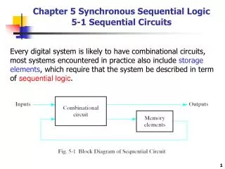
State Reduction and Assignment • In the design process of sequential circuits certain techniques are useful in reducing the circuit complexity • state reduction • state assignment • State reduction • Fewer states fewer number of flip-flops • m flip-flops 2m states • Example: m = 5 2m = 32 • If we reduce the number of states to 21 do we reduce the number of flip-flops?
0/0 a 0/0 1/0 0/0 0/0 b c 0/0 1/0 1/0 g d 0/0 e 1/1 1/1 1/1 f 0/0 1/1 Example: State Reduction Note that we use letters to designate the states for the time being
Example: State Reduction • What is important • not the states • but the output values the circuit generates • Therefore, the problem is to find a circuit • with fewer number of states, • but that produces the same output pattern for any given input pattern, starting with the same initial state
State Reduction Technique 1/7 0/0 a • Step 1: get a state table 1/0 b
State Reduction Technique 2/7 • Step 2: Inspect the state table for equivalent states • Equivalent states: Two states, • that produce exactly the same output • whose next states are identical • for each input combination
State Reduction Technique 3/7 • States “e” and “g” are equivalent • One of them can be removed
State Reduction Technique 4/7 • We keep looking for equivalent states
State Reduction Technique 5/7 • We keep looking for equivalent states
State Reduction Technique 6/7 • We stop when there are no equivalent states
State Reduction Technique 7/7 0/0 a 0/0 0/0 1/0 b 0/0 1/0 1/0 d 0/0 e We need two flip-flops 1/1 1/1
State Assignments 1/4 • We have to assign binary values to each state • If we have m states, then we need a code with minimum n bits, where n = log2m • There are different ways of encoding • Example: Eight states: S0, S1, S2, S3, S4, S5 , S6 , S7
State Assignments 2/4 • The circuit complexity depends on the state encoding (assignment) scheme • Previous example: binary state encoding
State Assignments 3/4 0/0 a • Gray encoding 0/0 0/0 1/0 b 0/0 1/0 0/0 1/0 d e 1/1
State Assignments 4/4 • One-hot encoding
Designing Sequential Circuits • Combinational circuits • can be designed given a truth table • Sequential circuits • We need, • state diagram or • state table • Two parts • flip-flops: number of flip-flops is determined by the number of states • combinational part: • output equations • flip-flop input equations
Design Process • Once we know the types and number of flip-flops, design process is reduced to design process of combinational circuits • Therefore, we can apply the techniques of combinational circuit design • The design steps • Given a verbal description of desired operation, derive state diagram • Reduce the number of states if necessary and possible • State assignment
Design Steps (cont.) • Obtain the encoded state table • Derive the simplified flip-flop input equations • Derive the simplified output equations • Draw the logic diagram • Example: Verbal description • “we want a (sequential) circuit that detects three or more consecutive 1’s in a string of bits” • Input: string of bits of any length • Output: • “1” if the circuit detects the pattern in the string • “0” otherwise
0 1 S0 S1/0 S2/0 S3/1 0 1 0 0 1 1 Example: State Diagram • Step 1: Derive the state diagram /0 Moore Machine
0 1 S0 S1/0 S2/0 S3/1 0 1 0 0 1 1 Synthesis with D Flip-Flops 1/5 • The number of flip-flops • Four states • ? flip-flops • State reduction • not possible in this case • State Assignment • Use binary encoding • S0 00 • S1 01 • S2 10 • S3 11 /0
0 1 S0 S1/0 S2/0 S3/1 0 0 0 1 Synthesis with D Flip-Flops 2/5 • Step 4: Obtain the state table /0 1 1
Synthesis with D Flip-Flops 3/5 • Step 5: Choose the flip-flops • D flip-flops • Step 6: Derive the simplified flip-flop input equations • Boolean expressions for DA and DB DA = Ax + Bx
Synthesis with D Flip-Flops 3/5 DB = Ax + B’x • Step 7: Derive the simplified output equations • Boolean expressions for y. y = AB
DA = Ax + Bx y = AB DB = Ax + B’x x DA A Q D C R y DB B Q D C R clock reset Synthesis with D Flip-Flops 5/5 • Step 8: Draw the logic diagram
S0 S1 S7 S2 S6 S3 S5 S4 Synthesis with T Flip-Flops 1/4 • Example: 3-bit binary counter with T flip-flops • 012 ... 7 0 1 2 How many flip-flops? • State assignments: • S0 000 • S1 001 • S2 010 • ... • S7 111 State Diagram
present state next state FF inputs A2 A1 A0 A2 A1 A0 T2 T1 T0 0 0 0 0 0 1 0 0 1 0 1 0 0 1 0 0 1 1 0 1 1 1 0 0 1 0 0 1 0 1 1 0 1 1 1 0 1 1 0 1 1 1 1 1 1 0 0 0 Synthesis with T Flip-Flops 2/4 • State Table
Synthesis with T Flip-Flops 3/4 • Flip-Flop input equations T2 = A1A0 T0 = 1 T1 = A0
A0 logic-1 T0 Q T C R A1 T1 Q T C R A2 T2 Q T clock C R reset Synthesis with T Flip-Flops 4/4 • Circuit T2 = A1A0 T1 = A0 T0 = 1
Present state Input next state Flip-flop inputs A B x A B JA KA JB KB 0 0 0 0 0 0 X 0 X 0 0 1 0 1 0 X 1 X 0 1 0 1 0 1 X X 1 0 1 1 0 1 0 X X 0 1 0 0 1 0 X 0 0 X 1 0 1 1 1 X 0 1 X 1 1 0 1 1 X 0 1 1 1 0 0 X 1 X 1 Synthesis with JK Flip-Flops 1/4 Q(t+1) = JQ’ + K’Q • State Table & JK FF Inputs X 0
Flip-flop inputs A B x A(t+1) B(t+1) JA KA JB KB 0 0 0 0 0 0 X 0 X 0 0 1 0 1 0 X 1 X 0 1 0 1 0 1 X X 1 0 1 1 0 1 0 X X 0 1 0 0 1 0 X 0 0 X 1 0 1 1 1 X 0 1 X 1 1 0 1 1 X 0 1 1 1 0 0 X 1 X 1 Synthesis with JK Flip-Flops 2/4 • Optimize the flip-flop input equations X 0 JA = Bx’ JB = x
Flip-flop inputs A B x A(t+1) B(t+1) JA KA JB KB 0 0 0 0 0 0 X 0 X 0 0 1 0 1 0 X 1 X 0 1 0 1 0 1 X X 1 0 1 1 0 1 0 X X 0 1 0 0 1 0 X 0 0 X 1 0 1 1 1 X 0 1 X 1 1 0 1 1 X 0 1 1 1 0 0 X 1 X 1 Synthesis with JK Flip-Flops 3/4 X 0 KA = Bx KB = (A x)’
JA = Bx’ KA = Bx JB = x KB = (A x)’ A Q J x C K B Q J clk C C K Synthesis with JK Flip-Flops 4/4 • Logic diagram Q D
S0 S1 S4 S2 S3 Unused States Modulo-5 counter
Example: Unused States 1/4 A(t+1) = B(t+1) = C(t+1) =
000 111 Present State Next State A B C A B C 001 100 0 0 0 0 0 1 0 0 1 0 1 0 0 1 0 0 1 1 010 011 0 1 1 1 0 0 1 0 0 0 0 0 1 1 0 0 1 0 1 1 1 1 0 0 101 110 Example: Unused States 2/4 A(t+1) = BC B(t+1) = B C C(t+1) = A’C’
Example: Unused States 3/4 • Not using don’t care conditions A(t+1) = A’BC B(t+1) = A’B’C + A’BC’ = A’(B C) C(t+1) = A’C’
111 000 110 101 001 100 010 011 A(t+1) = A’BC B(t+1) = A’(B C) C(t+1) = A’C’ Example: Unused States 4/4
th ts D Q tp, FF Sequential Circuit Timing 1/3 • It is important to analyze the timing behavior of a sequential circuit • Ultimate goal is to determine the maximum clock frequency clk
Combinational Circuit inputs outputs tp,COMB current state Flip-flop inputs Flip-flops Q D tp,FF ts clock C Sequential Circuit Timing 2/3 tp clk ts tp,FF tp,COMB tp= tp,FF+ tp,COMB+ts
Combinational Circuit inputs outputs tp,COMB current state Flip-flop inputs Flip-flops Q D tp,FF clock C Sequential Circuit Timing 2/3 tp clk ts tp,FF tp,COMB tp,FF+ tp,COMB>>th
tp clk ts tp,FF tp,COMB tp clk ts tp,FF tp,COMB Sequential Circuit Timing 3/3 • Minimum clock period (or maximum clock frequency)
Q D C B A B’ clk y x tp,NOT = 0.5 ns tp,XOR = 2.0 ns tp,FF = 2.0 ns tp,AND = ts = 1.0 ns th = 0.25 ns Example: Sequential Circuit Timing Find the longest path delay from external input to the output tp,XOR + tp,XOR = 2.0 + 2.0 = 4.0 ns
Q D C B A B’ clk y x tp,NOT = 0.5 ns tp,XOR = 2.0 ns tp,FF = 2.0 ns tp,AND = ts = 1.0 ns th = 0.25 ns Example: Sequential Circuit Timing Find the longest path delay in the circuit from external input to positive clock edge tp,XOR + tp,NOT = 2.0 + 0.5 = 2.5 ns
Q D C B A B’ clk y x tp,NOT = 0.5 ns tp,XOR = 2.0 ns tp,FF = 2.0 ns tp,AND = ts = 1.0 ns th = 0.25 ns Example: Sequential Circuit Timing Find the longest path delay from positive clock edge to output tp,FF + tp,XOR = 2.0 + 2.0 = 4.0 ns
Q D C B A B’ clk y x tp,NOT = 0.5 ns tp,XOR = 2.0 ns tp,FF = 2.0 ns tp,AND = ts = 1.0 ns th = 0.25 ns Example: Sequential Circuit Timing Find the longest path delay from positive clock edge to the flip-flop input tp,FF + tp,AND + tp,XOR + tp,NOT= 2.0 + 1.0 + 2.0 + 0.5 = 5.5 ns
Q D C B A B’ clk y x tp,NOT = 0.5 ns tp,XOR = 2.0 ns tp,FF = 2.0 ns tp,AND = ts = 1.0 ns th = 0.25 ns Example: Sequential Circuit Timing Determine the maximum frequency of operation of the circuit in megahertz tp = tp,FF + tp,AND + tp,XOR + tp,NOT + ? = 2.0 + 1.0 + 2.0 + 0.5 + 1.0 = 6.5 ns fmax = 1/tp = 1/(6.5×10-9) 154 MHz
S0 S3 x1 Q D C S1 S2 x0 tp,XOR = 2.0 ns Q D C tp,FF = 2.0 ns x0’ ts = 1.0 ns Example Binary encoding tp = tp,FF + tp,XOR + ts = 2.0 + 2.0 + 1.0 = 5.0 ns fmax = 1/tp = 1/(5.0×10-9) 200 MHz
y0 Q Q Q Q D D D D C C C C tp,FF = 2.0 ns y1 ts = 1.0 ns y2 y3 Example: One-Hot-Encoding S0 0001 S1 0010 S2 0100 S3 1000 tp = tp,FF + ts = 2.0 + 1.0 = 3.0 ns fmax = 1/tp = 1/(3.0×10-9) 333 MHz