INTRODUCTION TO LOGIC DESIGN Chapter 5 Synchronous Sequential Logic
INTRODUCTION TO LOGIC DESIGN Chapter 5 Synchronous Sequential Logic. gürtaç yemişçioğlu. OUTLINE OF CHAPTER 5. Analysis of Clocked Sequential Circuits. Latches. Sequential Circuits. Flip-flop. State Reduction a nd Assignment. Design Procedure. 5 .1 SEQUENTIAL circuits.

INTRODUCTION TO LOGIC DESIGN Chapter 5 Synchronous Sequential Logic
E N D
Presentation Transcript
INTRODUCTION TOLOGIC DESIGNChapter 5Synchronous SequentialLogic gürtaçyemişçioğlu
OUTLINE OF CHAPTER 5 Analysis of Clocked Sequential Circuits Latches Sequential Circuits Flip-flop State Reduction and Assignment Design Procedure INTRODUCTION TO LOGIC DESIGN
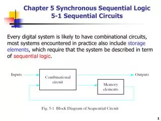
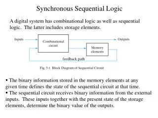
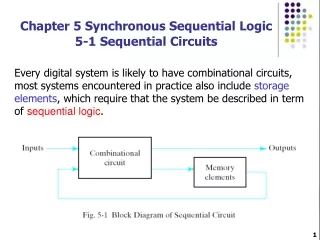
Combinational Circuit Inputs Outputs MemoryElements SEQUENTIAL CIRCUITS • Every digital system is likely to have combinational circuits. • Most systems encountered in practice also include storage elements, which require that the system be described in terms of sequential logic. INTRODUCTION TO LOGIC DESIGN
SEQUENTIAL CIRCUITS • The storage elements are devices capable of storing binary information. • The binary information stored in these elements at any given time defines the state of the sequential circuit at that time. • The sequential circuit receives binary information from external inputs. • These inputs, together with the present state of the storage elements, determine the binary value of the outputs. INTRODUCTION TO LOGIC DESIGN
SEQUENTIAL CIRCUITS • They also determine the condition for changing the state in the storage elements. • A sequential circuit is specified by a time sequence of inputs, output, and internal states. INTRODUCTION TO LOGIC DESIGN
SEQUENTIAL CIRCUITS • There are two main types of sequential circuits. • Their classification depends on the timing of their signals. INTRODUCTION TO LOGIC DESIGN
Combinational Circuit Inputs Outputs MemoryElements SEQUENTIAL CIRCUITS • Asynchronous Sequential Circuit • The behaviour of the circuit depends upon the input signals at any instant of time and the order in which the inputs change. INTRODUCTION TO LOGIC DESIGN
SEQUENTIAL CIRCUITS • Asynchronous Sequential Circuit • In gate – type asynchronous systems, the storage elements consist of logic gates whose propagation delay provides the required storage. • Thus, an asynchronous sequential circuit may be regarded as a combinational circuit with feedback. • Because of the feedback among logic gates, an asynchronous sequential circuit may become unstable at times. INTRODUCTION TO LOGIC DESIGN
Combinational Circuit Inputs Outputs Flip-flops SEQUENTIAL CIRCUITS • Synchronous Sequential Circuit • The behaviour can be defined from the knowledge of its signals at discrete instants of time. Clock INTRODUCTION TO LOGIC DESIGN
SEQUENTIAL CIRCUITS • Synchronous Sequential Circuit • Employs signals that affect the storage elements only at discrete instants of time. • Synchronisation is achieved by a timing device called a clock generator. • Provides a periodic train of clock pulses. • Clock pulses are distributed throughout the system in such a way that storage elements are affected only with the arrival of each pulse. INTRODUCTION TO LOGIC DESIGN
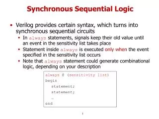
SEQUENTIAL CIRCUITS • Synchronous Sequential Circuit • In practice, the clock pulses are applied with other signals that specify the required change in the storage elements. • Circuits that use clock pulses in the inputs of storage elements are called clocked sequential circuits. • The storage elements used in clocked sequential circuits are called flip – flops. • A flip – flop is a binary storage device capable of storing one bit of information. INTRODUCTION TO LOGIC DESIGN
LATCHES • Latches are the basic circuits from which all flip – flops are constructed. • Although latches are useful for storing binary information and for the design of asynchronous sequential circuits. • They are not practical for use in synchronous sequential circuits. INTRODUCTION TO LOGIC DESIGN
LATCHES • SR Latch 1 0 Set State 1 0 0 1 Hold State 1 0 0 1 Reset State Hold State 0 1 0 0 1 0 Invalid State 0 0 INTRODUCTION TO LOGIC DESIGN
LATCHES • SR Latch No change Reset Set Invalid Invalid Set Reset No change INTRODUCTION TO LOGIC DESIGN
LATCHES • SR Latch with Control Input No change No change Reset Set Invalid INTRODUCTION TO LOGIC DESIGN
LATCHES • D Latch (D = Data) • One way to eliminate the undesirable condition of the indeterminate state in the SR latch is to ensure that inputs S and R are never equal to 1 at the same time. • D latch has two inputs • D (data) - directly goes to the S input and its complement is applied to the R input. • C (control) INTRODUCTION TO LOGIC DESIGN
LATCHES Timing Diagram • D Latch (D = Data) C D Q t No change Reset Set Output may change INTRODUCTION TO LOGIC DESIGN
LATCHES Timing Diagram • D Latch (D = Data) C D Q No change Reset Set Output may change INTRODUCTION TO LOGIC DESIGN
LATCHES • D Latch (D = Data) • The D latch has an ability to hold data in its internal storage. • It is suited for use as a temporary storage for binary information. • This circuit is often called transparent latch. • The output follow changes in the data input as long as the control input is enabled. INTRODUCTION TO LOGIC DESIGN
FLIP – FLOPS • Flip – flops are constructed in such a way to make D latches operate properly when they are part of a sequential circuit that employs a common clock. • The problem with the latch is that • It responds to a change in the level of a clock pulse. • Positive level response in the control input allows changes, in the output when the D input changes while the control pulse stays at logic 1. • The key to the proper operation of a flip – flop is • to trigger it only during a signal transition. INTRODUCTION TO LOGIC DESIGN
C CLK Positive Edge CLK Negative Edge FLIP – FLOPS • Controlled latches are level – triggered • Flip-Flops are edge – triggered INTRODUCTION TO LOGIC DESIGN
FLIP – FLOPS • There are two ways that a latch can be modified to form a flip – flop. • Employ two latches in a special configuration that • isolates the output of the flip – flop from being affected while its input is changing. • Produce a flip – flop that triggers only during a signal transition. • From 0 to 1 or from 1 to 0 only. • Disabled during the rest of the clock pulse duration. INTRODUCTION TO LOGIC DESIGN
D Latch (Master) D C D Latch (Slave) D C D Q Q Q CLK FLIP – FLOPS • Master – Slave D flip – flops Master Slave CLK Looks like it is negative edge-triggered D QMaster QSlave INTRODUCTION TO LOGIC DESIGN
FLIP – FLOPS • Edge-Triggered D Flip – Flop • Two latches respond to the external D (data) and CLK (clock inputs). • Third latch provides the outputs for the flip – flop. INTRODUCTION TO LOGIC DESIGN
FLIP – FLOPS • Edge-Triggered D Flip – Flop • When CLK = 0, S = 1 and R = 1.Output = present state. • If D = 0, when CLK 1 • R changes to 0 • Flip – flop goes to the RESET state. • Q = 0. INTRODUCTION TO LOGIC DESIGN
FLIP – FLOPS • Edge-Triggered D Flip – Flop • If D changes when CLK = 1 then • R remains at 0. • Flip – flop is locked out • Unresponsive to further changes in the input. • When CLK 0, • R 1 • Placing the output latch in the quiescent condition. • No change in the output. INTRODUCTION TO LOGIC DESIGN
FLIP – FLOPS • Edge-Triggered D Flip – Flop • If D = 1 when CLK = 0 1, • S changes to 0. • Circuit goes to SET state • Q = 1. • Any change in D while CLK = 1 does not affect the output. INTRODUCTION TO LOGIC DESIGN
FLIP – FLOPS • Edge-Triggered D Flip – Flop • When CLK in the positive-edge-triggered flip – flop • Makes positive transition • The value of D is transferred to Q. • Makes negative transition • Does not affect the output. • Steady CLK 1 or 0 • Does not affect the output. INTRODUCTION TO LOGIC DESIGN
FLIP – FLOPS • Edge-Triggered D Flip – Flop • The timing of the response of a flip – flop to input data and clock must be taken into consideration when using edge – triggered flip - flops. • There is a minimum time, called setup time, for which the D input must be maintained at a constant value prior to the occurrence of the clock transition. • There is a minimum time, called hold time, for which the D input must not change after the application of the positive transition of the clock. INTRODUCTION TO LOGIC DESIGN
D Q Q Q D Q FLIP – FLOPS • Edge-Triggered D Flip – Flop Positive Edge Dynamic input Negative Edge INTRODUCTION TO LOGIC DESIGN
FLIP – FLOPS • The most economical and efficient flip – flop constructed is the edge – triggered D flip – flop. • It requires smallest number of gates. • Other types of flip – flops can be constructed by using the D flip – flop and external logic. • JK flip – flops • T flip - flops INTRODUCTION TO LOGIC DESIGN
FLIP – FLOPS • There are three operations that can be performed with a flip – flop: • Set it to 1 • Reset it to 0 • Complement its output INTRODUCTION TO LOGIC DESIGN
FLIP – FLOPS • JK Flip – Flop • Performs all three operations. • When J = 1, sets the flip – flop to 1. • When K = 1, resets the flip – flop to 0. D = JQ’ + K’Q INTRODUCTION TO LOGIC DESIGN
FLIP – FLOPS • JK Flip – Flop Operation 1 • When J = 1 and K = 0, • D = 1.Q’ + 1.Q (Post2b) • D = Q’ + Q (Post5a) • D = 1 • Next clock edge sets the output to 1. D = JQ’ + K’Q INTRODUCTION TO LOGIC DESIGN
FLIP – FLOPS • JK Flip – Flop Operation 2 • When J = 0 and K = 1, • D = 0.Q’ + 0.Q (Theo2b) • D = 0 + 0 • D = 0 • Next clock edge sets the output to 0. D = JQ’ + K’Q INTRODUCTION TO LOGIC DESIGN
FLIP – FLOPS • JK Flip – Flop Operation 3 • When J = 1 and K = 1, • D = 1.Q’ + 0.Q (Post2b) • D = Q’ + 0 .Q (Theo2b) • D = Q’ + 0 (Post2a) • D = Q’ • Next clock edge complements the output. D = JQ’ + K’Q INTRODUCTION TO LOGIC DESIGN
FLIP – FLOPS • JK Flip – Flop • When J = 0 and K = 0, • D = 0.Q’ + 1.Q (Theo2b) • D = 0 + 1 .Q (Post2b) • D = 0 + Q (Post2a) • D = Q • Next clock edge the output is unchanged. D = JQ’ + K’Q INTRODUCTION TO LOGIC DESIGN
Q J Q K FLIP – FLOPS • JK Flip – Flop D = JQ’ + K’Q INTRODUCTION TO LOGIC DESIGN
Q J T Q K FLIP – FLOPS • T (toggle) Flip – Flop • Complementing flip – flop. • Can be obtained from a JK flip – flop. • When inputs J and K are tied together. • Useful for designing binary counters. C D = JQ’ + K’Q D = TQ’ + T’Q = T Q INTRODUCTION TO LOGIC DESIGN
Q J T Q K FLIP – FLOPS • T (toggle) Flip – Flop • When T = 0 (J = K = 0) • A clock edge does not change the output. • When T = 1 (J = K = 1) • A clock edge complements the output. C D = JQ’ + K’Q D = TQ’ + T’Q = T Q INTRODUCTION TO LOGIC DESIGN
Q D Q T FLIP – FLOPS • T (toggle) Flip – Flop • Can be constructed with a D flip – flop and an XOR gate. • When T = 0 then D = Q • No change in the output. • When T = 1 then D = Q’ • Output complements C D = TQ’ + T’Q = T Q INTRODUCTION TO LOGIC DESIGN
Q Q D T Q Q Q J T Q T K FLIP – FLOPS • T (toggle) Flip – Flop C C C (a) From JK Flip – Flop (b) From D Flip – Flop (c) Graphic Symbol INTRODUCTION TO LOGIC DESIGN
Q FLIP – FLOPS • Flip – Flop Characteristics Table D Q Reset Set Q(t+1) = D INTRODUCTION TO LOGIC DESIGN Q(t+1) =TQ
Q FLIP – FLOPS • Flip – Flop Characteristics Table No change Reset Set Toggle J Q K Q(t+1) = JQ’ + K’Q INTRODUCTION TO LOGIC DESIGN
Q FLIP – FLOPS • Flip – Flop Characteristics Table T Q No change Toggle Q(t+1) =T ⊕ Q INTRODUCTION TO LOGIC DESIGN
FLIP – FLOPS • Some flip – flops have asynchronous inputs that are used to force the flip – flop to a particular state independent of the clock. • The input that sets the flip – flop to 1 is called preset. • The input that clears the flip – flop to 0 is called clear or direct reset. • When power is on in a digital system, the state of the flip flop is unknown. INTRODUCTION TO LOGIC DESIGN
FLIP – FLOPS • When power is on in a digital system, the state of the flip flop is unknown. • The direct inputs are useful for bringing all flip – flops in the system to a known starting state prior to the clocked operation. INTRODUCTION TO LOGIC DESIGN