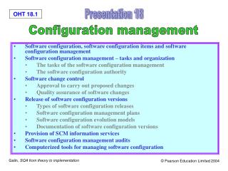
Configuration
Configuration. Process of loading bitstream of a design into the configuration memory. Bitstream is the transmission of characters at the fixed rate of speed. Parallel and Serial configuration modes. Configuration File.

Configuration
E N D
Presentation Transcript
Process of loading bitstream of a design into the configuration memory. • Bitstream is the transmission of characters at the fixed rate of speed. • Parallel and Serial configuration modes. Mirjana Stojanovic mirus@ptt.yu
Configuration File • Data are generated by the Xilinx development software. • Frames of data are stored in configuration file. • PROM is not required for storing data before loading. Mirjana Stojanovic mirus@ptt.yu
Modes • Four configuration modes: # Slave Serial mode # Master Serial mode # Slave Parallel mode # Boundary-scan mode • Modes are selected with configuration mode pins (M2,M1,M0). • Mode pins are default to a logic High if left unconnected. Mirjana Stojanovic mirus@ptt.yu
Signals • Two kinds of pins that are used in configuration process: # dedicated - for specific configuration-related functions # other pins - after configuration serve as general purpose I/Os • Dedicated pins: M2, M1, M0, CCLK, PROGRAM, DONE, TDI, TDO, TMS, TCK. Mirjana Stojanovic mirus@ptt.yu
The Process • Phases of configuration process: #1 Initiating the configuration #2 Configuration memory clear #3 Loading data frames #4 Start-up Mirjana Stojanovic mirus@ptt.yu
Phase #1: Initiating the Configuration • Two different ways to initiate the configuration process: applying power to the device or asserting the PROGRAM input pin. • Once in user operation, the device can be re-configured by pulling the PROGRAM pin Low. • The device acknowledges the beginning of the configuration process by driving the DONE Low. Mirjana Stojanovic mirus@ptt.yu
Phase #2: Clearing Configuration Memory • The device indicates that clearing the configuration memory is in progress by driving INIT Low. • The delay of configuration – holding either PROGRAM or INIT Low. • The device indicates that the memory is completely clear by driving INIT High. • Mode pins are sampled on Low-to-High transition of INIT . Mirjana Stojanovic mirus@ptt.yu
Phase #3:Loading Configuration Data • When INIT goes High, loading of the configuration data frames begins. • The sequence of operations in this phase is determined by the selected configuration mode. • The CRC (Cyclic Redundancy Checking) algorithm is used to verify bitstream integrity during configuration. • If error occurs the device pulls INIT low. Mirjana Stojanovic mirus@ptt.yu
Phase #4:Start-up • A match of CRC values initiates the Start-up sequence. The device performs four operations: #1 The assertion of DONE #2 The release of the Global Three State net (GTS) #3 The Negation of Global Set Reset (GSR) #4 The assertion of Global Write Enable (GWE) Mirjana Stojanovic mirus@ptt.yu
Start-up sequence lasts eight cycles, CO-C7. • The four operations can be selected to switch on any cycle C1-C6 through settings in the Xilinx development software. Mirjana Stojanovic mirus@ptt.yu
GTS,GSR, and GWE events are made conditional upon the DONE pin going high in the configuration options. • Sync-to-done is important for a daisy chain of multiple FPGAs in serial mode. Mirjana Stojanovic mirus@ptt.yu
Serial Modes • The FPGA is configured by loading one bit per CCLK cycle. • The MSB of each configuration data byte is always written to the DIN pin first. Mirjana Stojanovic mirus@ptt.yu
Slave Serial Mode • FPGA in Slave Serial Mode passively receives CCLK as an input from an external agent (e.g. a microprocessor or second FPGA in master mode). • Multiple FPGAs in Slave Serial mode can be daisy-chained for configuration from a single source. • After an FPGA is configured, data for the next device is routed to the DOUT pin. • Configuration must be delayed until INIT pins of all daisy-chained FPGAs are High. Mirjana Stojanovic mirus@ptt.yu
Master Serial Mode • In Master Serial mode, the CCLK output of the FPGA drives a Xilinx PROM which feeds a serial stream of configuration data to the FPGA’s DIN input. • An oscillator internal to the FPGA is used to generate the configuration clock (CCLK). • While the first 60 bytes of the configuration data are being loaded, the CCLK frequency is always 2.5 MHz. • When the ConfigRate bits are loaded into the FPGA, the frequency changes to the selected ConfigRate. • ConfigRate is 4MHz by default although it can range from 4 to 60MHz. Mirjana Stojanovic mirus@ptt.yu
Slave Parallel Mode • The fastest configuration option. • Byte-wide data is written into the FPGA. • BUSY flag is provided for controlling the flow of data at a clock frequency above 50MHz. • Controlling agent of the Slave Parallel interface can be processor, microcontroller or CPLD . • Controlling agent provides byte-wide configuration data, CCLK,CS and WRITE. Mirjana Stojanovic mirus@ptt.yu
The MSB must be routed to the D0 input on the FPGA. • If BUSY is asserted (High) by the FPGA, the data must be held until BUSY goes Low. • Multiple Spartan-II FPGAs can be configured using the Slave Parallel mode, and be made to start-up simultaneously. • Sync-to-DONE start-up timing is used to ensure that the start-up sequence does not begin until the FPGAs have been loaded. Mirjana Stojanovic mirus@ptt.yu
Write • Write operations send packets of byte-wide configuration data into the FPGA. • User holds WRITE and CS Low through the sequence of write operations. Mirjana Stojanovic mirus@ptt.yu
Write: #1 driving data onto D0-D7. The data source should be enabled while CS is low and WRITE is high. #2 on the rising edge of CCLK: if BUSY is low , the data is accepted on this clock. If BUSY is high the acceptance will occur on the first clock after BUSY goes low and data must be held until. #3 repeat steps 1 and 2 until all the data has been sent. #4 de-assert CS and WRITE. • If CCLK is slower than FCCNH , the data can simply be entered into the FPGA every CCLK cycle. Mirjana Stojanovic mirus@ptt.yu
Abort • To abort a configuration during a write sequence, de-assert WRITE while holding CS Low. • The abort operation is initiated at the rising edge of CCLK. • The device will remain BUSY until the aborted operation is complete. Mirjana Stojanovic mirus@ptt.yu
Boundary-Scan Mode • Configuration being done entirely through the IEEE 1149.1 Test Access Port. • Used to test the interconnections between devices on a printed circuit board. • Architecture includes 4- or 5- wired TAP, the TAP controller , the instruction register, the instruction decoder, the boundary-scan register and bypass register. • Configuration and readback via TAP is always available. • The boundary-scan mode simply locks out the other modes. Mirjana Stojanovic mirus@ptt.yu
Steps required to configure the FPGA through the boundary-scan port: #1 Load the CFG_IN instruction into the boundary-scan instruction register (IR) #2 Enter the Shift-DR (SDR) state #3 Shift a standard configuration bitstream into TDI #4 Return to Run-Test-Idle (RTI) #5 Load the JSTART instruction into IR #6 Enter the SDR state #7 Clock TCK through the sequence (the length is programmable) #8 Return to RTI Mirjana Stojanovic mirus@ptt.yu
Readback • Readback is the process of reading out all the data in the internal configuration memory. • Verifying that the current configuration data is correct. • Reading the current state of all internal CLB and IOB registers as well as current LUT RAM and block RAM values. • Available only through the Slave Parallel and boundary-scan interfaces. • Used for hardware debugging and functional verification. Mirjana Stojanovic mirus@ptt.yu


