Download
1 / 25
250 likes | 450 Views
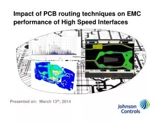
Impact of PCB routing techniques on EMC performance of High Speed Interfaces. Presented on: March 13 th , 2014. Impact of PCB routing techniques on EMC performance of HS Interfaces Johnson Controls Incorporated. Building Efficiency

E N D
Impact of PCB routing techniques on EMC performance of High Speed Interfaces Presented on: March 13th, 2014
Impact of PCB routing techniques on EMC performance of HS InterfacesJohnson Controls Incorporated Building Efficiency • A leading provider of equipment, controls and services for heating, ventilating, air-conditioning, refrigeration, and security systems for buildings. Automotive Experience • A global leader in automotive seating, overhead systems, door and instrument panels, and interior electronics. Power Solutions • Global leader in lead-acid automotive batteries and advanced batteries for Start-Stop, hybrid and electric vehicles. • Incorporated in 1885 • NYSE: JCI • No. 67 on U.S. Fortune 500 • Headquarters–Milwaukee, WI, United States 2 Johnson Controls
Impact of PCB routing techniques on EMC performance of HS interfacesDesign challenges in modern electronic modules • New product features • Innovative functions • Modern yet familiar user interface • Visual and functional appeal • New challenging product requirements • Functional requirements • EMC requirements • Mechanical and Thermal • Demanding business targets • Timing, cost and quality
Impact of PCB routing techniques on EMC performance of HS interfacesDesign aids available for engineers • Modern measurement equipment • Simulation Tools • Experienced engineering and support staff • Professional publications and training materials
Impact of PCB routing techniques on EMC performance of HS interfacesEMC guidelines from professional publications • EMC: Impact of vias in high speed signals • EMC: GND plane size and presence of guard traces • Sometimes you get mixed signals on what is the right design approach.
Impact of PCB routing techniques on EMC performance of HS interfacesSignal-Integrity guidelines from professional publications • Microstip vs. Stripline – Propagation delays, losses and crosstalk dilemma • Again you can see mixed messages. • What if you try to optimize design in both Signal Integrity and EMC areas?
Impact of PCB routing techniques on EMC performance of HS interfacesCase study • Purpose: Evaluate EMC performance of different clock net routing topologies, • in order to identify optimal solution for EMC and SI&TA performance. • Experiment #1: • Microstrip (MS) vs Stripline (SL) routing • Stripline with two vias vs MS/SL with eight vias (*) • Experiment #2: • Using Gnd vs Power as a reference plane (*) • Experiment #3: • MS top to bottom layers transitionwith and without GND stitching vias • Experiment #4: • MS with nominal ZO vs MS with Zo increased by 15% • Experiment #5: • Stripline (SL) vs MS with guard traces • (*) – assuming close coupling for signals and planes (under 4 mils or 100 um)
Impact of PCB routing techniques on EMC performance of HS interfacesCase study Circuit topology implementation for test clock net PCB stackup • IC oscillator operated at 12 MHz, Clock Net length was 6 cm • All CLK cases (except for CLK7) - signal routing use Layer1 and Layer 3 with Layer 4 being void • CLK7 - signal routing use Layer1 and Layer 4 with Layer 3 being a power plane
Impact of PCB routing techniques on EMC performance of HS interfacesCase study Experiment #1 • Vertical view of Clock Nets Experiment #1 Experiment #3 Experiment #2 Experiment #2 Experiment #4 Experiment #5 Experiment #5 Horizontal view of Clock Nets
Impact of PCB routing techniques on EMC performance of HS interfacesEMC evaluation Results – RF Scan • RF scan at 84 MHz • All clock topologies RF scan at 300 MHz CLK1, CLK2 and CLK3
Impact of PCB routing techniques on EMC performance of HS interfacesEMC evaluation methods – Conducted Emissions Block diagram of CE evaluation method Actual setup with DUT
Impact of PCB routing techniques on EMC performance of HS interfacesEMC evaluation methods – Radiated Emissions CiSPR25 Block diagram of RE evaluation method Actual setup with DUT
Impact of PCB routing techniques on EMC performance of HS interfacesEMC evaluation Results – Experiment #1 – Conducted Emissions - Raw Data CLK1 CLK2 Combined Plots CLK3
Impact of PCB routing techniques on EMC performance of HS interfacesEMC evaluation Results – Experiment #1 – Radiated Emissions - Raw Data CLK1 CLK2 Combined Plots RE CLK3
Impact of PCB routing techniques on EMC performance of HS interfacesEMC evaluation Results – Experiment #1 • Stripline net topology shown lowest emissions, for both CE and RE cases • Microstrip net topology shown highest emissions, for both CE and RE cases • Stripline with 8 vias does not perform worse than Microstrip (CE and RE)
Impact of PCB routing techniques on EMC performance of HS interfacesEMC evaluation Results – Experiment #2 • Stripline referenced to a Power Plane does not perform any worse then stripline referenced to a Ground Plane (both CE and RE) • (*) – spacing between power and ground planes is 4 mils (100 um)
Impact of PCB routing techniques on EMC performance of HS interfacesEMC evaluation Results – Experiment #3 • Microstrip which transitions between Top and Bottom layers (8 vias) does not show EMC improvements when ground Stitching Ground vias were added (RE & CE)
Impact of PCB routing techniques on EMC performance of HS interfacesEMC evaluation Results – Experiment #4 • Microstrip with characteristic impedance increased by 15% have shown small to moderate increase in EMC emissions (RE & CE)
Impact of PCB routing techniques on EMC performance of HS interfacesEMC evaluation Results – Experiment #5 • Microstrip with ground guard traces has shown small improvement in EMC performance (RE & CE) over Microstrip, but it does not perform better than Stripline
Impact of PCB routing techniques on EMC performance of HS interfacesSignal-Integrity and Timing Properties – Trace Topology Impedance • Variation of the average trace impedance was within 8% from means for all nets with exception for CLK17 (planned impedance increase by 15%) • Presence of multiple vias results in substantial increase of maximum impedance variation in the given net (CLK3, CLK5, CLK6) • (*) - Average trace impedance measured last three quarters length of the clock net
Impact of PCB routing techniques on EMC performance of HS interfacesSignal-Integrity and Timing Properties – Time Domain Response • Average rise time distortion had shown strong differentiation between clock net topology cases, but its value has remained low (under 3%) • Clock net topology has little impact on worst case rise time distortion measurement (*) – Rise time was evaluated between CMOS VIL & VIH levels (30% & 70% of VCC)
Impact of PCB routing techniques on EMC performance of HS interfacesEMC evaluation results - Conclusions Results: • EMC emissions (RE&CE) of Stripline were always lower than Microstrip, even with presence of 8 vias (performance no worse than MS) • EMC emissions (RE&CE) have not been affected by changing signal reference from ground to power plane (closely spaced planes 100 um) • EMC emission performance of Microstrip transitioning between top and bottom layers was much worse, than that of a Stripline, addition of ground stitching vias has not affected EMC performance • Increase of Zo has resulted in increase of EMC emissions (RE&CE) • EMC emissions of Microstrip with guard trace were slightly lower than of Microstrip, but worse than Stripline • Presence of vias and reference plane changes affects negatively transition time, but for clock frequencies under 200 MHz its impact is negligible • Evaluation case: • Single driver and single receiver with a series termination, 6 cm long trace • 8 layer PCB with closely spaced layers (100 um) • 12 MHz low jitter source was used with rise time of 1.4 ns (20% to 80 %)
Impact of PCB routing techniques on EMC performance of HS interfacesAppendix 1 • Publications referenced in the presentation: • Modeling and Analysis of Return Path Discontinuity Caused by Vias using the 3-Conductor Model, A. Ege Engin, IEEE transactions 2003 • Reduction of Printer Circuit Board Radiated Emissions, Frank B.J. Leferink • Summary of Design Techniques, TBD • High-Speed Board Layout Guidelines, Altera Application Note 224, August 2009 • EMC Design Guideline for Microcontroller Board Layout, Infineon Application Note 1999-07 • Dramatic Noise Reduction using Guard Traces with Optimized Shorting Vias, Eric Bogatin,DesignCon 2013
Impact of PCB routing techniques on EMC performance of HS interfacesAppendix 2 – Simulation setup 33Ω Clock Trace Load 6.8 pF Source (Gaussian Pulse) Simulation Settings: Tool : CST Microwave Studio Boundary Condition : Open add space Back ground Space : 10mm in all directions Frequency : 0 - 3 GHz Meshing : Hexahedral Mesh cells : ~ 1.5 Million Solver : Time domain Frequency Samples : 3001 Broad band e-field (far-field) probes 1m away – In all 6 directions Note: Simulation setup does not evaluate the same type of EMC performance which was evaluated via testing. Purpose of those simulations is to evaluate e-field radiation pattern in Z direction above the PCB.
Impact of PCB routing techniques on EMC performance of HS interfacesAppendix 2 – Simulation results Experiment 1 and Experiment 2 • Simulation results confirm that emissions from stripline routing topology (CLK2) are smaller than that from microstrip (CLK1) • Simulation results indicate that there is small variation between emission from microstrip transitioning between top and bottom layers, in cases when ground stitching vias were present or absent