Download
1 / 4
40 likes | 80 Views
PCB routing was a tough job tough however we have mentioned the best tips for High speed PCB routing. For more information call us today.

E N D
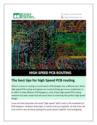
The best tips for high Speed PCB routing When it comes to routing a circuit board a PCB designer has a difficult task. When high speed PCB routing and signals are involved things get more complicated. In an effort to help different PCB designers, a list of best high speed PCB routing practices has been made that will assist them in achieving that perfect high-speed design. It was not that long when the word “high speed” didn’t exist in the vocabulary of PCB designers. However these days, it seems to be just opposite. At that time, the only concern was all about putting the puzzle pieces together and strategizing
your way through a physical board layout. But what with high speed design? Now here there is a bunch of invisible forces to worry about, things like electromagnetic interference which is also known as EMI, crosstalk, signal reflection and etc. To handle the extra advanced computing needs of these devices high speed circuitry is required in dense PCB designs. Other than that is the RF portion of these devices which increases the complexity of their small yet powerful circuit boards. However to successfully design these boards, PCB designers need to balance the requirements of a board that has both high speed and RF PCB routing on it. What are the key points of high speed and RF PCB routing? Once you start working on a printed circuit board with high speed and RF circuitry in it, there will be a lot of specific design rules that you will have to observe. You also have to remember however that no matter what, you are still designing a circuit board. This clearly means that in addition to the new design parameters that you will be working on with; you will still have to follow all of the regular rules of High speed PCB routing and design. These will include the features below:
Thermal Issues with components that run hot. High speed circuitry tends to generate more heat, and you may need to keep thermal issues in mind now more than ever. You should make sure that your board it getting cooled the way that is should be. You should keep in mind the basic PCB design rules for digital, analog, power and mixed signal technologies. Just because you need more room for high speed traces or RF shielding doesn’t mean that you can ignore you regular PCB design spacing rules and squeeze things together.
Design for Manufacturing rules or DFM rules. You have got a much bigger problem on your head if your design can’t be built because of basic DFM rules violations. This also includes designing your board for both assembly and test (DFA and DFT). Click here: https://www.crimpcircuits.com/blog/the-best-tips- for-high-speed-pcb-routing/