Download
1 / 59
590 likes | 816 Views
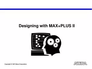
Ch. 4 Introduction to MAX+PLUS II. 이 상 훈 경남대학교 전기전자공학부. 단원목차. 1. What is a PLD? 2. Programming PLDs using MAX+PLUS II 3. Graphic Design File 4. Compiling MAX+PLUS II Files 5. Hierarchical Design 6. Text Design File(VHDL) 7. Creating a Physical Design. Programmable Logic Device (PLD).

E N D
Ch. 4Introduction to MAX+PLUS II 이 상 훈 경남대학교 전기전자공학부
단원목차 1. What is a PLD? 2. Programming PLDs using MAX+PLUS II 3. Graphic Design File 4. Compiling MAX+PLUS II Files 5. Hierarchical Design 6. Text Design File(VHDL) 7. Creating a Physical Design
Programmable Logic Device (PLD) • Supplied with no predetermined logic function. • Programmed by user to implement any digital logic function. • Requires specialized computer software for design and programming.
Advantages of Using PLDs • Saves on number of chips used. (refer to example 4.1) • Saves on different types of chips used. • Shortens the design process. • Creates design flexibility.
Complex PLD (CPLD) • A PLD that has several programmable sections with internal interconnections between the sections. • In effect, CPLD is several interconnected PLDs on a single chip.
PLD Programming • Requires specialized computer software. • Programmed through a series of steps known as the PLD Design Cycle. • One program is Altera’s MAX+PLUS II.
PLD Design Cycle - 1 • Design entry – enter the circuit. • Simulation – verify that the circuit outputs correctly respond to the inputs. • Compilation – create the required design information for programming the CPLD.
PLD Design Cycle - 2 • Fitting – determine which portions of the CPLD to assign as circuitry for the required design. • Programming – configures the CPLD to perform the desired logic function.
Altera Target Devices • CPLDs used for implementing designs. • MAX7000S family – EPM7128SLC84-7, a non-volatile CPLD. • FLEX10K family – EPF10K20RC240-4, a volatile CPLD.
Volatile vs. Non-Volatile • Volatile – information (programming) is only available as long as power is applied to the device. • Non-Volatile – information (programming) is available even after power is removed and then reapplied.
CPLD Design Entry • Two general methods. • 1. Schematic, or graphic, entry. • 2. Text based entry.(VHDL, Verilog HDL)
MAX+PLUS II Graphic Entry • Uses a Graphic Design File (.gdf) in which the digital design is entered as a schematic. • Shows components and their inter-connections, as well as the input and output names of the circuit. • See Figure 4.3
Figure 4.3 • Majority Vote Circuit
Creating a Graphic Design File • Uses schematic entry. • MAX+PLUS II generates other files required for programming. • All the files represent a project. • See Figure 4.6
MAX+PLUS II Project • A set of files associated with a particular PLD design. • All operations to create program files for a PLD are performed on a project. • Always keep track of what the current project is.
Creating MAX+PLUS II Graphic Design Files • First, Save the file to the proper folder. • Second, Set Project to Current File. • Figure 4.8
Entering Components • Use cursor to set the component location and press left mouse button. • Use right mouse button to enable entry menu. • Choose Enter Symbol. • Figure 4.9
Enter Symbol Menu • Allows basic components to be entered by name or selected from a library. • Basic components are called primitives. • Each copy of a component is called an instance. • Figure 4.10
Moving and Aligning Symbols • Symbols can be moved by highlighting them, using the left mouse button, then dragging them to the desired location. • Figure 4.11
Moving and Aligning Symbols • Figure 4.12 • Figure 4.13
Connecting Components • Components are connected by clicking over one end of one component and dragging a line to one end of a second component. Figure 4.14
Assigning Pin Names • Inputs and outputs must be assigned names. • Double-click the pin name (e.g. INPUT_VCC) to highlight it and type in the assigned name. Figure 4.17
Target Device • Before compiling, a target device must be specified. • To select a target device, use the Assign menu, followed by Device. • Figure 4.18, 4.19
Target Device • Device Dialog Box
Compile Options • Design Doctor checks for good design practice. • Timing SNF Extractor creates the file needed to perform timing simulation. • Smart Recompile allows use of previously compiled portions that have not changed.
Compile Options • Figure 4.20 • MAX+PLUS II • Compiler Settings • Figure 4.21 • MAX+PLUS II • Compiler Operation
Compile Messages • Three types of message. • One, Info (green text), for information only. • Two, Warning (blue text), to identify potential, but nonfatal, problems. • Three, Error (red text), to identify design flaws that render the design unusable.
Compile Files • Generates a Programmer Object File (.pof) for non-volatile CLPDs. • Generates a SRAM Object File (.sof) for volatile CPLDs.
Hierarchical Design • A PLD design ordered in layers or levels. • The top level contains components that are themselves complete designs. • Lower level components may have even lower level designs embedded within them.
Default Symbol • A graphic symbol used to represent a PLD design as a block. • Shows only the design’s inputs and outputs. • Used as a component in a hierarchical design.
Text Based Entry • Uses Hardware Description Language (HDL). • A more powerful design technique than graphic entry.
Hardware Description Language • A computer language used to design circuits with text-based descriptions of the circuits. • VHDL (VHSIC Hardware Description Language) is the industry-standard language used for programming PLDs.
VHDL History • Developed by defense contractors as a standard for programming circuits. • Currently defined by IEEE Std. 1076-1993.
Basic VHDL Rules • Rules of construction are called “syntax.” • Not case-sensitive, but style guidelines suggest that keywords, devices, constants and primitives are capitalized. • Comments are delineated by double dashes before the text. • Comments are not compiled.
VHDL Structure • Requires entity declaration and an architecture body. • The entity defines the design inputs and outputs. • The architecture defines the relationship between inputs, outputs and the internal signals.
VHDL Entity • Defines the external aspects of the function. • Each input or output is a port. • The type of port is defined by mode. • Fig 4.28 • Graphical Representation of a • VHDL Design Entity
Types of Port Modes • IN refers to a port used only for input. • OUT refers to a port used only for output. • INOUT refers to a bidirectional port. • BUFFER refers to a special case of OUT that has a feedback connection back into the CPLD logic.
Types of Port Modes • Fig 4.29 • VHDL Port Modes • Fig 4.30 • BUFFER and OUT Modes
Port Types • Type defines what values the port is allowed to have. • Can be single or multi-bit definitions.
Single Bit Port Types • BIT can have a value of ‘0’ or ‘1’. • STD_LOGIC can have one of nine values. • INTEGER can have whole number values.
STD_LOGIC Type Definitions • Possible values include:‘U’– uninitialized ‘X’– forcing unknown‘0’– forcing 0 ‘1’– forcing 1‘Z’– high impedance ‘W’– weak unknown‘L’– weak 0 ‘H’– weak 1‘-’– don’t care. • Usually use ‘X’, ‘0’, ‘1’, and ‘Z’.
Multi-bit Port Types • BIT_VECTOR can have multiple instances of 0 or 1. • STD_LOGIC_VECTOR can have multiple instances of U, X, 0, 1, Z, W, L, H, and -. • Vector means a group of signals treated as a single multi-bit variable.
VHDL Architecture • Defines the internal aspects, how the inputs and outputs behave with respect to one another and with respect to other internal signals or functions. • Uses operators to define the logical relationships.
Architecture Operators • <= assigns the value of the right hand side of an equation to the left hand side. • Logical operators are assigned by name, such as ‘and’ and ‘or’.
Order of Precedence • All logical operators have equal order of precedence. • Use parenthesis to make the order of precedence explicit.
Concurrent Signal Assignment • Concurrent means simultaneous. • The order in which signals in an architecture body are evaluated does not depend on the order in which they are written. • A change in one input common to several circuits affects all the circuits at the same time.
Example - Majority Vote2 LIBRARY ieee; USE ieee.std_logic_1164.ALL; ENTITY maj_vot2 IS PORT( a, b, c : IN STD_LOGIC; y : OUT STD_LOGIC); END maj_vot2; ARCHITECTURE majority OF maj_vot2 IS BEGIN y <= (a and b) or (b and c) or (a and c); END majority;
Example 4.3 – 2-Line-to-4-Line Decoder • Multiple possible solutions. • Can be described using individual inputs or using vectors. • Figure 4.31
Example 4.3 – Vector Definitions • Can specify by defining the upper and lower limits – (3 downto 0), (0 to 3), (4 downto 1) and (1 to 4). • Can specify by using selected signal assignment statement.