Download
1 / 36
370 likes | 581 Views
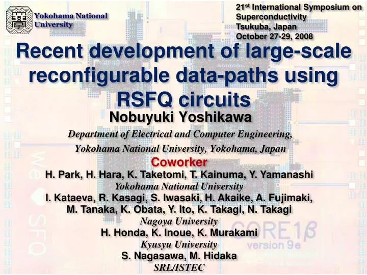
21 st International Symposium on Superconductivity Tsukuba, Japan October 27-29, 2008. Yokohama National University. Recent development of large-scale reconfigurable data-paths using RSFQ circuits. Nobuyuki Yoshikawa Department of Electrical and Computer Engineering,

E N D
21st International Symposium on Superconductivity Tsukuba, Japan October 27-29, 2008 Yokohama National University Recent development of large-scale reconfigurable data-paths using RSFQ circuits Nobuyuki Yoshikawa Department of Electrical and Computer Engineering, Yokohama National University, Yokohama, Japan Coworker H. Park, H. Hara, K. Taketomi, T. Kainuma, Y. Yamanashi Yokohama National University I. Kataeva, R. Kasagi, S. Iwasaki, H. Akaike, A. Fujimaki, M. Tanaka, K. Obata, Y. Ito, K. Takagi, N. Takagi Nagoya University H. Honda, K. Inoue, K. Murakami Kyusyu University S. Nagasawa, M. Hidaka SRL/ISTEC
Outline of This Talk • Background • Architecture • Target system • Component developments • Floating-point adders/multipliers (FPA/FPU) • 2 x 2 RDP • New process and cell library • Road map • Summary
Demand on High-Performance Computer Calculation amount of electronic structure of molecules using the molecular orbital method O(N4) 600 TB of ERI calculations composed of a lot of product-sum operations A molecule with 1000 atoms
Breakdown of Moore’s Law Trends of the clock frequency of recent microprocessors 5 Pentium 4 3 1.1x / year Clock frequency [GHz] 1.6x / year Xeon Celeron 1 Pentium III 0.8 0.6 0.4 http://www.intel.com/ 0.2 1998 1999 2000 2001 2002 2003 2004
Problem in High-Performance Computersand Our Approach • Large power consumption • Memory wall problem (Single Flux Quantum circuits + new architecture) solves these problems Josephson junction F0 = h/2e = 2.07 mV. ps
Large-Scale Reconfigurable Data-Path (LSRDP) using RSFQ Circuits A lot of FPUs + Reconfigurable network The data are directly transferred between FPUs. Reduction of memory wall problem N. Takagi et al. IEICE Technical Report, SCE2006-36, January 2007.
Example of Application of LSRDP Electron repulsion integral calculations of molecular orbit while (I < 1000): tei(4,4,4,4)=(((3+2*p*(4*PAx*PBx+PBx**2+PAx**2*(1+2*p*PBx**2)))*(3+2*q*(4*QCx*QDx+QDx**2+QCx**2*(1+2*q*QDx**2)))*f(0,t))/(p**2*q**2)+(4*(3+2*p*(4*PAx*PBx+PBx**2+PAx**2*(1+2*p*PBx**2)))*PQx*(QCx+QDx)*(3+2*q*QCx*QDx)*f(1,t))/(p*q*(p+q))(4*(PAx+PBx)*(3+2*p*PAx*PBx)*PQx*(3+2*q*(4*QCx*QDx+QDx**2+QCx**2*(1+2*q*QDx**2)))*f(1,t))/(p*q*(p+q))(8*(PAx+PBx)*(3+2*p*PAx*PBx)*(QCx+QDx)*(3+2*q*QCx*QDx)*(((p+q)*f(1,t))+2*p*PQx**2*q*f(2,t)))/(p*q*(p+q)**2)+(2*(3+2*p*(4*PAx*PBx+PBx**2+PAx**2*(1+2*p*PBx**2)))*(3+q*(QCx**2+4*QCx*QDx+QDx**2))*(((p+q)*f(1,t))+2*p*PQx**2*q*f(2,t)))/(p*q**2*(p+q)**2)+(2*(3+p*(PAx**2+4*PAx*PBx+PBx**2))*(3+2*q*(4*QCx*QDx+QDx**2+QCx**2*(1+2*q*QDx**2)))*(((p+q)*f(1,t))+2*p*PQx**2*q*f(2,t)))/(p**2*q*(p+q)**2)+(4*(3+2*p*(4*PAx*PBx+PBx**2+PAx**2*(1+2*p*PBx**2)))*PQx*(QCx+QDx)*(3*(p+q)*f(2,t)+2*p*PQx**2*q*f(3,t)))/(q*(p+q)**3)\+(8*(3+p*(PAx**2+4*PAx*PBx+PBx**2))*PQx*(QCx+QDx)*(3+2*q*QCx*QDx)*(3*(p+q)*f(2,t)+2*p*PQx**2*q*f(3,t)))/(p*(p+q)**3)(8*(PAx+PBx)*(3+2*p*PAx*PBx)*PQx*(3+q*(QCx**2+4*QCx*QDx+QDx**2))*(3*(p+q)*f(2,t)+2*p*PQx**2*q*f(3,t)))/(q*(p+q)**3)(4*(PAx+PBx)*PQx*(3+2*q*(4*QCx*QDx+QDx**2+QCx**2*(1+2*q*QDx**2)))*(3*(p+q)*f(2,t)+2*p*PQx**2*q*f(3,t)))/(p*(p+q)**3)+((3+2*p*(4*PAx*PBx+PBx**2+PAx**2*(1+2*p*PBx**2)))*(3*(p+q)**2*f(2,t)+4*p*PQx**2*q*(3*(p+q)*f(3,t)+p*PQx**2*q*f(4,t))))/(q**2*(p+q)**4)(8*(PAx+PBx)*(3+2*p*PAx*PBx)*(QCx+QDx)*(3*(p+q)**2*f(2,t)+4*p*PQx**2*q*(3*(p+q)*f(3,t)+p*PQx**2*q*f(4,t))))/(q*(p+q)**4)(8*(PAx+PBx)*(QCx+QDx)*(3+2*q*QCx*QDx)*(3*(p+q)**2*f(2,t)+4*p*PQx**2*q*(3*(p+q)*f(3,t)+p*PQx**2*q*f(4,t))))/(p*(p+q)**4)+(4*(3+p*(PAx**2+4*PAx*PBx+PBx**2))*(3+q*(QCx**2+4*QCx*QDx+QDx**2))*(3*(p+q)**2*f(2,t)+4*p*PQx**2*q*(3*(p+q)*f(3,t)+p*PQx**2*q*f(4,t))))/(p*q*(p+q)**4)+((3+2*q*(4*QCx*QDx+QDx**2+QCx**2*(1+2*q*QDx**2)))*(3*(p+q)**2*f(2,t)+4*p*PQx**2*q*(3*(p+q)*f(3,t)+p*PQx**2*q*f(4,t))))/(p**2*(p+q)**4)(4*p*(PAx+PBx)*(3+2*p*PAx*PBx)*PQx*(15*(p+q)**2*f(3,t)+4*p*PQx**2*q*(5*(p+q)*f(4,t)+p*PQx**2*q*f(5,t))))/(q*(p+q)**5)+(8*(3+p*(PAx**2+4*PAx*PBx+PBx**2))*PQx*(QCx+QDx)*(15*(p+q)**2*f(3,t)+4*p*PQx**2*q*(5*(p+q)*f(4,t)+p*PQx**2*q*f(5,t))))/(p+q)**5+(4*PQx*q*(QCx+QDx)*(3+2*q*QCx*QDx)*(15*(p+q)**2*f(3,t)+4*p*PQx**2*q*(5*(p+q)*f(4,t)+p*PQx**2*q*f(5,t))))/(p*(p+q)**5)(8*(PAx+PBx)*PQx*(3+q*(QCx**2+4*QCx*QDx+QDx**2))*(15*(p+q)**2*f(3,t)+4*p*PQx**2*q*(5*(p+q)*f(4,t)+p*PQx**2*q*f(5,t))))/(p+q)**5+(8*(PAx+PBx)*(QCx+QDx)*(15*(p+q)**3*f(3,t)+30*p*PQx**2*q*(p+q)*(3*(p+q)*f(4,t)+2*p*PQx**2*q*f(5,t))8*p**3*PQx**6*q**3*f(6,t)))/(p+q)**6+(2*(3+p*(PAx**2+4*PAx*PBx+PBx**2))*(15*(p+q)**3*f(3,t)30*p*PQx**2*q*(p+q)*(3*(p+q)*f(4,t)+2*p*PQx**2*q*f(5,t))+8*p**3*PQx**6*q**3*f(6,t)))/(q*(p+q)**6)+(2*(3+q*(QCx**2+4*QCx*QDx+QDx**2))*(15*(p+q)**3*f(3,t)30*p*PQx**2*q*(p+q)*(3*(p+q)*f(4,t)+2*p*PQx**2*q*f(5,t))+8*p**3*PQx**6*q**3*f(6,t)))/(p*(p+q)**6) 787 MUL, 261 ADD, 69 FUNC I = I+1: Data-flow graph mapped to the LSRDP
LSRDP Architecture: Suitable for RSFQ Circuits • Data flow in one direction. No loop structure. • Need high throughput. Latency is not so important. • Suitable for bit-serial processing. • Reduced requirement on memory band width. • High switching activity. Heating is serious in semiconductor circuits
Application Fields of LSRDP Processors • Molecular orbit calculation • Diffusion equation • Wave equation • Poisson equation etc.
Target System:10-TFLOPS RSFQ-LSRDP Computer 4.2 K SFQ 0.5um process CMOS CPU (1chip) ORN 2TB memory module (FB-DIMM [DDR3@1333MHz, 128GB] ×16 modules) ... FPU SFQ RDP (32FPU×32chips) (4GFLOPS/FPU) ORN : : : : ... ORN SFQ Streaming Buffer (64Kb×2chips) ... ORN SB 1024FPU@MCM (34chips)×4MCM : : : ... : SMAC SMAC SMAC Memory band width per MCM:256GB/s (=16GB/s ×16 channels)
Organization of the Project • Profs. K. Murakami, H. Honda (Kyushu Univ.) • LSRDP architecture, compiler, algorithm • Profs. N. Takagi, K. Takagi (Nagoya Univ.) • CAD for logic design, arithmetic circuits • Prof. N. Yoshikawa (Yokohama National Univ.) • RSFQ-FPU chip, cell library • Profs. A. Fujimaki, H. Akaike (Nagoya Univ.) • Network, RSFQ-LSRDP chip, cell library • Dr. S. Nagasawa (SRL) • Advanced process
Component Development • Floating-point adder (FPA) • Floating-point multiplier (FPM) • Operand routing network (ORN) • 2 x 2 LSRDP prototype
Floating-Point Numbers S: Sign E: Exponent F: Significand or Fraction (-1)S×F×2E Example (single precision, 32 bit): 1.101×24 0 11000011 10100000000000000000000 Data format in IEEE754 standard E(8 bit) S(1bit) F(23 bit)
Bit-Serial Floating-Point Calculation Two bit-serial data-paths are used for the calculation of significand and exponent. nf LSB MSB Significand ne LSB MSB Sign Exponent t
Timing Parameters in Bit-Serial Calculation Output Input (clock) Operation Unit (clock) (data) (data) Time Input 2 Input 3 Input 1 Output 1 Output Input MSB MSB LSB LSB MSB MSB MSB MSB LSB LSB LSB LSB (clock) Input (data) C. Minimum interval A. Skew (clock) Output (data) B. Latency
Floating-Point Addition: Example +( 1.110 × 22) + -( 1.010 × 24) Subtraction of exponents. Alignment of significands. Addition (or subtraction) of two significands. Production of the sign of the result. Normalization of result. Rounding. +( 0.01110 × 24) - ) +( 1.010 × 24) +(11.00110 × 24) -( 0.11010 × 24) -( 1.101 × 23)
Block Diagram of Bit-Serial FPA • Align significand • & Rounding (2) Addition (or subtraction) (3) Normalization Shifter of A Significand of A Adder & Subtractor Fa Normalizer Significand of Result Shifter of B Significand of B Fb Effective Operation Comparator of magnitude Result of Operation Shift value A > B Controller MUX Sa Amount of Correction Separator circuit Sing of Result Sb Result of “A-B” Exponent & Sign of A Normalizer & Sign and Exponent‘s Combine circuit Subtractor Ea Buffer Exponent & Sign of B Exponent & Sign of Result Eb Buffer : Data signals : Control signals
Chip Photograph of Half-Precision FPA Normalizer Shifter of A 1mm Adder & Subtractor Controller Shifter Register of Significands Normalizer • Half-precision FPA • Minimum interval: 12 clocks ( nf + 1) • Latency: 23 clocks ( 2nf + 1) • Operating frequency: 20 GHz • Performance: 1.67 GFLOPs • # of JJs : 11700 JJs • Power consumption: 3.5 mW • Size: 6.76 ×4.96mm2 Clock Generator Shifter Register for Confirmation Shifter Register of Exponent and Sign Shifter of B *SRL Nb 2.5 kA/cm2 standard process Shifter Register for Confirmation *nf : bit length of significand
DC Bias Margin of Each Component Circuits @20GHz Shifter_A Shifter_B Adder Normalizer of significand Normalizer of exponent Controller of shifter Controller of shifter and adder
Floating-Point Multiplier S: SignE: Exponent F: Fraction • Significand part is calculated by a systolic-array multiplier. (-1)S×F×2E • Exponent part is calculated by a bit-serial adder. • Zf=XfYf E(8 bit) S(1bit) F(23 bit) Ze=Xe+Ye
Systolic-Array Multiplier • Composed of 1D array of 1-b processing element (PE). • Small hardware cost: ∝(bit length) • High throughput : ~ 1/(bit length) Input Output MSB MSB LSB LSB
Clock Generator Chip Photograph ofHalf-Precision FPM Multiplier Shifter Register Normalizer Shifter Register Adder and Normalizer 1mm • Half-precision FPM • Minimum interval: 12 clocks ( nf + 1) • Latency: 11 clocks (nf ) • Operating frequency: 25 GHz • Performance: 2.1 GFLOPs • # of JJs : 11044 JJs • Power consumption: 3.5 mW • Size: 6.22 ×3.78 mm2 *SRL Nb 2.5 kA/cm2 standard process *nf : bit length of significand
Test Result of FPM@25GHz MSB LSB FX : 11010110111 EX: 11001 FY: 11001010011 EY: 01101 FXY: 10101001110 EXY: 11000 (10) [Calculation of exponent part ] (-2) (10) + (-2) + 1 = 9 Carry from fraction part EX EY Correct operation was confirmed at high speed. Maximum operating frequency: 31.5 GHz
Clock Generator Summary of Half-Precision FPUs Multiplier Shifter Register Normalizer FPA nf : bit length of fraction part Shifter Register Normalizer Normalizer 1mm Shifter of A Adder & Subtractor Controller Shifter Register of Significands Normalizer Clock Generator FPM Shifter Register for Confirmation Shifter Register of Exponent and Sign Shifter of B 1mm Shifter Register for Confirmation
Device Structure of Nb 10-layer Fabrication Process Active layer Including JJ and R Main GP and CPL 2nd PTL layer 1st PTL layer DC Power layer Bias pillar 10 kA/cm2 Nb process
Jc: 10 kA/cm2 bc = 2
Design of Bit-Serial Half Adder using a New Cell Library Logic simulation results of bit-serial half adder Jc: 10 kA/cm2 bc = 2
On-Chip High-Speed Test Results of Bit-Serial Half Adder Clock Generator Bit-Serial Adder Shift Register for Input Shift Register for Output Jc: 10 kA/cm2 bc = 2
Road Map of RSFQ LSRDP Processor 10 TFLOPS LSRDP system development 40 kA/cm2 Process 100 GHz FPU & LSRDP prototype FPA Normalizer 10 kA/cm2 Process 60 GHz FPU & LSRDP prototype Shifter of A Adder & Subtractor Controller Shifter Register of Significands Normalizer 2.5 kA/cm2 Process Clock Generator 25GHz FPU/RDP Shifter Register for Confirmation Shifter Register of Exponent and Sign 2014 - 2007 2008 2009 2010 2011 2012 2013 Shifter of B Shifter Register for Confirmation
Summary • Our target is to make a fundamental technology for high-end supercomputers based on large-scale reconfigurable data-path (LRDP) architecture. • Some key components were designed and implemented using standard Nb process, and their correct operations were demonstrated. • Half-precision RSFQ FPA and FPU • Operand routing network (ORN) • 2 x 2 RDP • Structure of the SRL advanced II process was determined and a new cell library is under development. • 85 GHz operation of bit-serial half-adder was demonstrated.