Download

1 / 38
430 likes | 627 Views
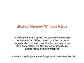
Flipping Bits in Memory Without Accessing Them. DRAM Disturbance Errors. Yoongu Kim Ross Daly, Jeremie Kim, Chris Fallin, Ji Hye Lee, Donghyuk Lee, Chris Wilkerson, Konrad Lai, Onur Mutlu. DRAM Chip. Row of Cells. Wordline. Row. Victim Row. Row. Aggressor Row. V LOW. V HIGH.

E N D
Flipping Bits in Memory Without Accessing Them DRAM Disturbance Errors Yoongu Kim Ross Daly, Jeremie Kim, Chris Fallin, Ji Hye Lee, Donghyuk Lee, Chris Wilkerson, Konrad Lai, Onur Mutlu
DRAM Chip Row of Cells Wordline Row Victim Row Row Aggressor Row VLOW VHIGH Closed Opened Row Victim Row Row Repeatedly opening and closing a row induces disturbance errorsin adjacent rows
Quick Summary of Paper • We expose the existence and prevalence of disturbance errors in DRAM chips of today • 110 of 129 modules are vulnerable • Affects modules of 2010 vintage or later • We characterize the cause and symptoms • Toggling a row accelerates charge leakage in adjacent rows: row-to-row coupling • We prevent errors using a system-level approach • Each time a row is closed, we refresh the charge stored in its adjacent rows with a low probability
1. Historical Context 2. Demonstration (Real System) 3. Characterization (FPGA-Based) 4. Solutions
A Trip Down Memory Lane IBM’s patent on DRAM 1968 Intel commercializes DRAM (Intel 1103) 1971 • Suffered bitline-to-cell coupling Bitline Bitline “... this big fat metal line with full level signals running right over the storage node (of cell).” – Joel Karp (1103 Designer) Interview: Comp. History Museum Cell 2013 8um 6um 2014
A Trip Down Memory Lane IBM’s patent on DRAM 1968 Intel commercializes DRAM (Intel 1103) 1971 • Suffered bitline-to-cell coupling Earliest DRAM with row-to-row coupling 2010 We observe row-to-row coupling 2013 Intel’s patents mention “Row Hammer” 2014
Lessons from History • Coupling in DRAM is not new • Leads to disturbance errors if not addressed • Remains a major hurdle in DRAM scaling • Traditional efforts to contain errors • Design-Time: Improve circuit-level isolation • Production-Time: Test for disturbance errors • Despite such efforts, disturbance errors have been slipping into the field since 2010
1. Historical Context 2. Demonstration (Real System) 3. Characterization (FPGA-Based) 4. Solutions
How to Induce Errors x86 CPU DRAM Module DDR3 • Avoid cache hits • Flush X from cache • Avoid row hits to X • Read Y in another row 111111111 X 111111111 111111111 111111111 Y 111111111 111111111
How to Induce Errors x86 CPU DRAM Module DDR3 loop: mov (X), %eax mov (Y), %ebx clflush (X) clflush (Y) mfence jmp loop 001110111 111111111 X 1111 111111111 111111111 101111101 110001011 111111111 1111 Y 111111111 011011110 111111111
Number of Disturbance Errors • In a more controlled environment, we can induce as many as ten million disturbance errors • Disturbance errors are a serious reliability issue
Security Implications • Breach of memory protection • OS page (4KB) fits inside DRAM row (8KB) • Adjacent DRAM row Different OS page • Vulnerability: disturbance attack • By accessing its own page, a program could corrupt pages belonging to another program • We constructed a proof-of-concept • Using only user-level instructions
Mechanics of Disturbance Errors • Cause 1: Electromagnetic coupling • Toggling the wordline voltage briefly increases the voltage of adjacent wordlines • Slightly opens adjacent rows Charge leakage • Cause 2: Conductive bridges • Cause 3: Hot-carrier injection Confirmed by at least one manufacturer
1. Historical Context 2. Demonstration (Real System) 3. Characterization (FPGA-Based) 4. Solutions
Infrastructure PC FPGA Board Test Engine PCIe DRAM Ctrl
Temperature Controller Heater FPGAs FPGAs PC
Tested DDR3 DRAM Modules • Total: 129 • Vintage: 2008 – 2014 • Capacity: 512MB – 2GB CompanyA Company C Company B 54 32 43
Characterization Results • Most Modules Are at Risk • Errors vs. Vintage • Error = Charge Loss • Adjacency: Aggressor & Victim • Sensitivity Studies • Other Results in Paper
1. Most Modules Are at Risk Acompany C company Bcompany • 88% • (28/32) • 86% • (37/43) • 83% • (45/54) Up to 1.0×10⁷errors Up to 2.7×10⁶errors Up to 3.3×10⁵errors
2. Errors vs. Vintage First Appearance All modules from 2012–2013 are vulnerable
3. Error = Charge Loss • Two types of errors • ‘1’ ‘0’ • ‘0’ ‘1’ • A given cell suffers only one type • Two types of cells • True: Charged (‘1’) • Anti: Charged (‘0’) • Manufacturer’s design choice • True-cells have only ‘1’ ‘0’ errors • Anti-cells have only ‘0’ ‘1’ errors Errors are manifestations of charge loss
4. Adjacency: Aggressor & Victim Adjacent Adjacent Adjacent Non-Adjacent Non-Adjacent Note: For three modules with the most errors (only first bank) Most aggressors & victims are adjacent
5. Sensitivity Studies time Test Row 1 Test Row 2 ··· Test Row 0 Fill Module with Data Open Open ··· Find Errors in Module Refresh Periodically Access-Interval: 55–500ns ❶ ❷ Refresh-Interval: 8–128ms Data-Pattern: all ‘1’s, all ‘0’s, etc. ❸
❶Access-Interval (Aggressor) Not Allowed 500ns 55ns Note: For three modules with the most errors (only first bank) Less frequent accesses Fewer errors
5. Sensitivity Studies time Test Row 1 Test Row 2 ··· Test Row 0 Fill Module with Data Open Open ··· Find Errors in Module Refresh Periodically Access-Interval: 55–500ns ❶ ❷ Refresh-Interval: 8–128ms Data-Pattern: all ‘1’s, all ‘0’s, etc. ❸
❷ Refresh-Interval ~7x frequent 64ms Note: Using three modules with the most errors (only first bank) More frequent refreshes Fewer errors
5. Sensitivity Studies time Test Row 1 Test Row 2 ··· Test Row 0 Fill Module with Data Open Open ··· Find Errors in Module Refresh Periodically Access-Interval: 55–500ns ❶ ❷ Refresh-Interval: 8–128ms Data-Pattern: all ‘1’s, all ‘0’s, etc. ❸
❸ Data-Pattern Solid RowStripe 10x Errors ~Solid ~RowStripe 000000 111111 111111 000000 000000 111111 111111 000000 111111 000000 111111 000000 000000 000000 111111 111111 Errors affected by data stored in other cells
Naive Solutions ❶Throttle accesses to same row • Limit access-interval: ≥500ns • Limit number of accesses: ≤128K (=64ms/500ns) ❷ Refresh more frequently • Shorten refresh-interval by ~7x Both naive solutions introduce significant overhead in performanceand power
Characterization Results • Most Modules Are at Risk • Errors vs. Vintage • Error = Charge Loss • Adjacency: Aggressor & Victim • Sensitivity Studies • Other Results in Paper
6. Other Results in Paper • Victim Cells ≠ Weak Cells (i.e., leaky cells) • Almost no overlap between them • Errors not strongly affected by temperature • Default temperature: 50°C • At 30°C and 70°C, number of errors changes <15% • Errors are repeatable • Across ten iterations of testing, >70% of victim cells had errors in every iteration
6. Other Results in Paper (cont’d) • As many as 4 errors per cache-line • Simple ECC (e.g., SECDED) cannot prevent all errors • Number of cells & rows affected by aggressor • Victims cells per aggressor: ≤110 • Victims rows per aggressor: ≤9 • Cells affected by two aggressors on either side • Very small fraction of victim cells (<100) have an error when either one of the aggressors is toggled
1. Historical Context 2. Demonstration (Real System) 3. Characterization (FPGA-Based) 4. Solutions
Several Potential Solutions Cost • Make better DRAM chips Power, Performance • Refresh frequently Cost, Power • Sophisticated ECC Cost, Power, Complexity • Access counters
Our Solution • PARA: Probabilistic Adjacent Row Activation • Key Idea • After closing a row, we activate (i.e., refresh) one of its neighbors with a low probability: p = 0.005 • Reliability Guarantee • When p=0.005, errors in one year: 9.4×10⁻¹⁴ • By adjusting the value of p, we can provide an arbitrarily strong protection against errors
Advantages of PARA • PARA refreshes rows infrequently • Low power • Low performance-overhead • Average slowdown: 0.20% (for 29 benchmarks) • Maximum slowdown: 0.75% • PARA is stateless • Low cost • Low complexity • PARA is an effective and low-overhead solution to prevent disturbance errors
Conclusion • Disturbance errors are widespread in DRAM chips sold and used today • When a row is opened repeatedly, adjacent rows leak charge at an accelerated rate • We propose a stateless solution that prevents disturbance errors with low overhead • Due to difficulties in DRAM scaling, new and unexpected types of failures may appear
Flipping Bits in Memory Without Accessing Them DRAM Disturbance Errors Yoongu Kim Ross Daly, Jeremie Kim, Chris Fallin, Ji Hye Lee, Donghyuk Lee, Chris Wilkerson, Konrad Lai, Onur Mutlu