Download
1 / 9
90 likes | 131 Views
Explore how design impacts sensitivity, model gas penetration into 3D sensors, set Niobium oxide conductivity, analyze data from real samples, and more.

E N D
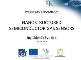
Projekt OPVK NANOTEAMNANOSTRUCTURED SEMICONDUCTOR GAS SENSORS Ing. Zdeněk Pytlíček 24.10.2014 Investice do rozvoje vzdělávání
Research Plan • How design affects a sensitivity • Model a gaspenetrationinto a 3D gas sensor • Set a conductivityof Niobium oxides • Model currentflow inthe3D gas sensor • Measure real samples from Sasha • Analyse obtained data Investice do rozvoje vzdělávání
Current DefinitionwithPerforatedElectrode Distance between pillars = 108 nm will be changed to 125 nm (all the dimensions in nanometers) dpillar = 60 nm sample for simulation = 5 m x 5 m => npillars ≈ 2500
Literature Review • [1] ThesisMANUSPIYA, H. Electrical Properties of Niobium Based Oxides-Ceramics and Single Crystal Fibers Grown by the Laser-Heated Pedestal Growth (LHPG) Technique. Engineering Science and Mechanics. The Pennsylvania State University, • [2] FABREGAT-SANTIAGO, F. et al. Mott-Schottky analysis of nanoporous semiconductor electrodes in dielectric state deposited on SnO2(F) conducting substrates. Journal of the Electrochemical Society, 2003, vol. 150, no. 6, pp. E293-E298. ISSN 0013-4651 • [3] ThesisBACH, D. EELS investigations of stoichiometric niobium oxides and niobium-based capacitors. Fakultät für Physik. Universität Karlsruhe, • [4] MOZALEV, A. et al. Formation-structure-properties of niobium-oxide nanocolumn arrays via self-organized anodization of sputter-deposited aluminum-on-niobium layers. Journal of Materials Chemistry C, 2014, vol. 2, no. 24, pp. 4847-4860. ISSN 2050-7526. • [5] DE SA, A. I. et al. Anodic oxidation and dielectric behaviour of aluminium-niobium alloys. Corrosion Science, 2006, vol. 48, no. 8, pp. 2203-2211. ISSN 0010-938X. • [6] LEE, S. et al. Single Crystalline NbO2 Nanowire Synthesis by Chemical Vapor Transport Method. Bulletin of the Korean Chemical Society, 2012, vol. 33, no. 3, pp. 839-842. ISSN 0253-2964. • [7] BELANGER, G. et al. Electron-Transport in Single-Crystals of Niobium Dioxide. Canadian Journal of Physics, 1974, vol. 52, no. 22, pp. 2272-2280. ISSN 0008-4204
Poděkování: Budování výzkumných týmů a rozvoj univerzitního vzdělávání výzkumných odborníků pro mikro- a nanotechnologie (NANOTEAM) CZ.1.07/2.3/.00/09.0224 Investice do rozvoje vzdělávání