Download
1 / 14
140 likes | 306 Views
Project Golden Mantle CMOS 8-Bit Analog-to-Digital Converter. Team Travis T ompkins Aaron K rizek Scott O strow. Advisor Dr. Joe Hoffbeck Dr. Peter Osterberg Industry Representative Mr. Howard Voorheis. Overview. Introduction Accomplishments Plans Issues/Concerns Demo

E N D
Project Golden MantleCMOS 8-Bit Analog-to-Digital Converter Team Travis Tompkins Aaron Krizek Scott Ostrow • Advisor • Dr. Joe Hoffbeck • Dr. Peter Osterberg • Industry Representative • Mr. Howard Voorheis University of Portland School of Engineering
Overview • Introduction • Accomplishments • Plans • Issues/Concerns • Demo • Conclusions Small...but FIERCE! University of Portland School of Engineering
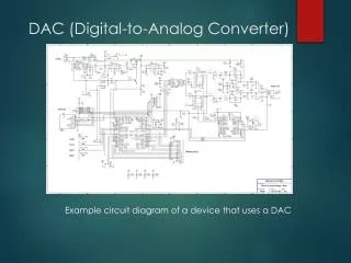
Introduction • 8-Bit Analog-to-Digital Converter “Tracking” ADC Architecture University of Portland School of Engineering
Introduction continued • Continuous time signal “coded” into stream of binary numbers • Key component in communication systems • - Cell Phones, Satellite Transmission, Digital Signal Processing University of Portland School of Engineering
Accomplishments • Theory of Operations and Approval Meeting • Layout determined • Solved CMOS/Macro Model cross connection problem • Core Components of Macro Model tested • Tracked AC and DC signals University of Portland School of Engineering
Pictures University of Portland School of Engineering
MOSIS CHIP Bonding pads: 40 Layout size: 2200 x 2200 microns; Area: 4.836 sq mm Packaging: DIP40 Maximum die size: 7366 x 7366 University of Portland School of Engineering
Bill of Materials University of Portland School of Engineering
Plans • Individual Component Testing • Prototype Integration • Begin Wire-Wrap Phase • Develop Logic to Prevent Looping in Macro Model University of Portland School of Engineering
Milestone Table University of Portland School of Engineering
Concerns/Issues • Timing Violations • Wire Wrap Techniques • Arrival of CMOS chip • Logic to prevent looping in Macro Model University of Portland School of Engineering
Detail: Timing Violation Solution University of Portland School of Engineering
Demo • Tracking Demo University of Portland School of Engineering
Conclusions • Introduction • Accomplishments • Plans • Issues/Concerns • Demo Small...but FIERCE! University of Portland School of Engineering