Chapter 1 Diodes
Chapter 1 Diodes. Outline of Chapter 1. 1.1 Introduction 1.2 Basic Semiconductor Concepts 1.3 The pn Junction 1.4 Analysis of diode circuits 1.5 Applications of diode circuits. 1.1 Introduction. The diode is the simplest and most fundamental nonlinear circuit element.

Chapter 1 Diodes
E N D
Presentation Transcript
Chapter 1Diodes SJTU Zhou Lingling
Outline of Chapter 1 1.1 Introduction 1.2 Basic Semiconductor Concepts 1.3 The pn Junction 1.4 Analysis of diode circuits 1.5 Applications of diode circuits SJTU Zhou Lingling
1.1 Introduction • The diode is the simplest and most fundamental nonlinear circuit element. • Just like resistor, it has two terminals. • Unlike resistor, it has a nonlinear current-voltage characteristics. • Its use in rectifiers is the most common application. SJTU Zhou Lingling
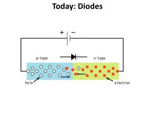
Physical Structure The most important region, which is called pn junction, is the boundary between n-type and p-type semiconductor. SJTU Zhou Lingling
Symbol and Characteristic for the Ideal Diode (a) diode circuit symbol; (b) i–vcharacteristic; (c) equivalent circuit in the reverse direction; (d) equivalent circuit in the forward direction. SJTU Zhou Lingling
Characteristics • Conducting in one direction and not in the other is the I-V characteristic of the diode. • The arrowlike circuit symbol shows the direction of conducting current. • Forward biasing voltage makes it turn on. • Reverse biasing voltage makes it turn off. SJTU Zhou Lingling
1.2 Basic Semiconductor Concepts • Intrinsic Semiconductor • Doped Semiconductor • Carriers movement SJTU Zhou Lingling
Intrinsic Semiconductor • Definition A crystal of pure and regular lattice structure is called intrinsic semiconductor. • Materials • Silicon---today’s IC technology is based entirely on silicon • Germanium---early used • Gallium arsenide---used for microwave circuits SJTU Zhou Lingling
Intrinsic Semiconductor(cont’d) Two-dimensional representation of the silicon crystal. The circles represent the inner core of silicon atoms, with +4 indicating its positive charge of +4q, which is neutralized by the charge of the four valence electrons. Observe how the covalent bonds are formed by sharing of the valence electrons. At 0 K, all bonds are intact and no free electrons are available for current conduction. SJTU Zhou Lingling
Intrinsic Semiconductor(cont’d) At room temperature, some of the covalent bonds are broken by thermal ionization. Each broken bond gives rise to a free electron and a hole, both of which become available for current conduction. SJTU Zhou Lingling
Intrinsic Semiconductor(cont’d) • Thermal ionization • Valence electron---each silicon atom has four valence electrons • Covalent bond---two valence electrons from different two silicon atoms form the covalent bond • Be intact at sufficiently low temperature • Be broken at room temperature • Free electron---produced by thermal ionization, move freely in the lattice structure. • Hole---empty position in broken covalent bond,can be filled by free electron, positive charge SJTU Zhou Lingling
Intrinsic Semiconductor(cont’d) • Carriers A free electron is negative charge and a hole is positive charge. Both of them can move in the crystal structure. They can conduct electric circuit. SJTU Zhou Lingling
Intrinsic Semiconductor(cont’d) • Recombination Some free electrons filling the holes results in the disappearance of free electrons and holes. • Thermal equilibrium At a certain temperature, the recombination rate is equal to the ionization rate. So the concentration of the carriers is able to be calculated. SJTU Zhou Lingling
Intrinsic Semiconductor(cont’d) • Carrier concentration in thermal equilibrium • At room temperature(T=300K) carriers/cm3 SJTU Zhou Lingling
Intrinsic Semiconductor(cont’d) Important notes: • has a strong function of temperature. The high the temperature is, the dramatically great the carrier concentration is. • At room temperature only one of every billion atoms is ionized. • Silicon’s conductivity is between that of conductors and insulators. Actually the characteristic of intrinsic silicon approaches to insulators. SJTU Zhou Lingling
Doped Semiconductor • Doped semiconductors are materials in which carriers of one kind predominate. • Only two types of doped semiconductors are available. • Conductivity of doped semiconductor is much greater than the one of intrinsic semiconductor. • The pn junction is formed by doped semiconductor. SJTU Zhou Lingling
Doped Semiconductor(cont’d) n type semiconductor • Concept Doped silicon in which the majority of charge carriers are the negatively charged electrons is called n type semiconductor. • Terminology • Donor---impurity provides free electrons, usually entirely ionized. • Positive bound charge---impurity atom donating electron gives rise to positive bound charge • carriers • Free electron---majority, generated mostly by ionized and slightly by thermal ionization. • Hole---minority, only generated by thermal ionization. SJTU Zhou Lingling
Doped Semiconductor(cont’d) A silicon crystal doped by a pentavalent element. Each dopant atom donates a free electron and is thus called a donor. The doped semiconductor becomes n type. SJTU Zhou Lingling
Doped Semiconductor(cont’d) p type semiconductor • Concept Doped silicon in which the majority of charge carriers are the positively charged holes is called p type semiconductor. • Terminology • acceptor---impurity provides holes, usually entirely ionized. • negatively bound charge---impurity atom accepting hole give rise to negative bound charge • carriers • Hole---majority, generated generated mostly by ionized and slightly by thermal ionization. • Free electron---minority, only generated by thermal ionization. SJTU Zhou Lingling
Doped Semiconductor(cont’d) A silicon crystal doped with a trivalent impurity. Each dopant atom gives rise to a hole, and the semiconductor becomes p type. SJTU Zhou Lingling
Doped Semiconductor(cont’d) Carrier concentration for n type • Thermal equilibrium equation • Electric neutral equation SJTU Zhou Lingling
Doped Semiconductor(cont’d) Carrier concentration for p type • Thermal equilibrium equation • Electric neutral equation SJTU Zhou Lingling
Doped Semiconductor(cont’d) Because the majority is much great than the minority, we can get the approximate equations shown below: for n type for p type SJTU Zhou Lingling
Doped Semiconductor(cont’d) • Conclusion • Majority carrier is only determined by the impurity, but independent of temperature. • Minority carrier is strongly affected by temperature. • If the temperature is high enough, characteristics of doped semiconductor will decline to the one of intrinsic semiconductor. SJTU Zhou Lingling
Doped Semiconductor(cont’d) • Doping compensation n type semiconductor is generated by donor diffusion, then injecting acceptor into the specific area(assuming ) forms p type semiconductor. The boundary between n and p type semiconductor is the pn junction. This is the basic step for VLSI fabrication technology. NA ND SJTU Zhou Lingling
Carriers Movement There are two mechanisms by which holes and free electrons move through a silicon crystal. • Drift--- The carrier motion is generated by the electrical field across a piece of silicon. This motion will produce drift current. • Diffusion--- The carrier motion is generated by the different concentration of carrier in a piece of silicon. The diffused motion, usually carriers diffuse from high concentration to low concentration, will give rise to diffusion current. SJTU Zhou Lingling
Drift and Drift Current • Drift • Drift velocities • Drift current densities Where are the constants called mobility of holes and electrons respectively. SJTU Zhou Lingling
Drift and Drift Current • Total drift current density • Resistivity SJTU Zhou Lingling
Drift and Drift Current • Resistivities for doped semiconductor * Resistivities are inversely proportional to the concentration of doped impurities. • Temperature coefficient(TC) TC for resistivity of doped semiconductor is positive due to negative TC of mobility For n type For p type SJTU Zhou Lingling
Drift and Drift Current • Resistivity for intrinsic semiconductor * Resistivity is inversely proportional to the carrier concentration of intrinsic semiconductor. • Temperature coefficient(TC) TC for resistivity of intrinsic semiconductor is negative due to positive TC of . SJTU Zhou Lingling
Diffusion and Diffusion Current • diffusion A bar of intrinsic silicon (a) in which the hole concentration profile shown in (b) has been created along the x-axis by some unspecified mechanism. SJTU Zhou Lingling
Diffusion and Diffusion Current where are the diffusion constants or diffusivities for hole and electron respectively. * The diffusion current density is proportional to the slope of the the concentration curve, or the concentration gradient. SJTU Zhou Lingling
Einstein Relationship Einstein relationship exists between the carrier diffusivity and mobility: Where VT is Thermal voltage. At room temperature, SJTU Zhou Lingling
1.3 pn Junction • The pn junction under open-circuit condition • I-V characteristic of pn junction • Terminal characteristic of junction diode. • Physical operation of diode. • Junction capacitance SJTU Zhou Lingling
pn Junction Under Open-Circuit Condition • Usually the pn junction is asymmetric, there are p+n and pn+. • The superscript “+” denotes the region is more heavily doped than the other region. SJTU Zhou Lingling
pn Junction Under Open-Circuit Condition Fig (a) shows the pn junction with no applied voltage (open-circuited terminals). Fig.(b) shows the potential distribution along an axis perpendicular to the junction. SJTU Zhou Lingling
Procedure of Forming pn Junction The procedure of forming pn the dynamic equilibrium of drift and diffusion movements for carriers in the silicon. In detail, there are 4 steps: • Diffusion • Space charge region • Drift • Equilibrium SJTU Zhou Lingling
Procedure of Forming pn Junction • diffusion • Both the majority carriers diffuse across the boundary between p-type and n-type semiconductor. • The direction of diffusion current is from p side to n side. SJTU Zhou Lingling
Procedure of Forming pn Junction • Space charge region • Majority carriers recombining with minority carriers results in the disappearance of majority carriers. • Bound charges, which will no longer be neutralized by majority carriers are uncovered. • There is a region close to the junction that is depleted of majority carriers and contains uncovered bound charges. • This region is called carrier-depletion region or space charge region. SJTU Zhou Lingling
Procedure of Forming pn Junction • Drift • Electric field is established across the space charge region. • Direction of electronic field is from n side to p side. • It helps minority carriers drift through the junction. The direction of drift current is from n side to p side. • It acts as a barrier for majority carriers to diffusion. SJTU Zhou Lingling
Procedure of Forming pn Junction • Equilibrium • Two opposite currents across the junction is equal in magnitude. • No net current flows across the pn junction. • Equilibrium conduction is maintained by the barrier voltage. SJTU Zhou Lingling
Junction Built-In Voltage The Junction Built-In Voltage • It depends on doping concentration and temperature • Its TC is negative. SJTU Zhou Lingling
Width of the Depletion Region Width of the Depletion Region: • Depletion region exists almost entirely on the slightly doped side. • Width depends on the voltage across the junction. SJTU Zhou Lingling
I-V Characteristics The diode i–v relationship with some scales expanded and others compressed in order to reveal details SJTU Zhou Lingling
I-V Characteristic Curve Terminal Characteristic of Junction Diodes • The Forward-Bias Region, determined by • The Reverse-Bias Region, determined by • The Breakdown Region, determined by SJTU Zhou Lingling
The pn Junction Under Forward-Bias Conditions • The pn junction excited by a constant-current source supplying a current I in the forward direction. • The depletion layer narrows and the barrier voltage decreases by V volts, which appears as an external voltage in the forward direction. SJTU Zhou Lingling
The pn Junction Under Forward-Bias Conditions Minority-carrier distribution in a forward-biased pn junction. It is assumed that the p region is more heavily doped than the n region; NA >>ND. SJTU Zhou Lingling
The pn Junction Under Forward-Bias Conditions Excess minority carrier concentration: • Exponential relationship • Small voltage incremental give rise to great incremental of excess minority carrier concentration. SJTU Zhou Lingling
The pn Junction Under Forward-Bias Conditions Distribution of excess minority concentration: Where are called excess-minority-carrier lifetime. SJTU Zhou Lingling
The pn Junction Under Forward-Bias Conditions The total current can be obtained by the diffusion current of majority carriers. SJTU Zhou Lingling