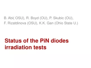
PIN DIODES
PIN DIODES. A SPECIAL APPLICATIONS DIODE. CONTENTS. INTRODUCTION & CONSTRUCTION OF PIN DIODE CHARACTRESTICS OF PIN DIODE OPERATION OF PIN DIODE GENERAL SPECIFICTIONS APPLICATIONS OF PIN DIODES. 1.1 Introduction & construction .


PIN DIODES
E N D
Presentation Transcript
PIN DIODES A SPECIAL APPLICATIONS DIODE
CONTENTS • INTRODUCTION & CONSTRUCTION OF PIN DIODE • CHARACTRESTICS OF PIN DIODE • OPERATION OF PIN DIODE • GENERAL SPECIFICTIONS • APPLICATIONS OF PIN DIODES
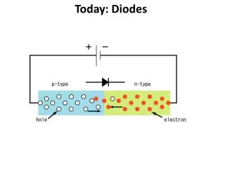
1.1 Introduction & construction 1.1.1: Introduction: - PIN diode is a type of special application diode which is made of three type of semi-conductor materials. 1.1.2: Construction:- A PIN diode is a diode with wide intrinsic region between a p-type semi-conductor and an n-type semi-conductor region. The p-type and n-type regions are typically very heavily doped they are used for ohmic contacts i.e., they have very low resistances.
1.1.4 PIN diode symbol:- The typical symbol used for PIN diode is shown below:
1.2 CHARACTERISTICS:- There are a number of PIN diode characteristics that set this diode apart from other forms of diode. 1.2.1 High breakdown voltage:- The wide depletion layer provided by the intrinsic layer ensures that PIN diodes have a high reverse breakdown characteristic. 1.2.2 Low capacitance:- Again the intrinsic layer increases the depletion region width. As the capacitance of a capacitor reduces with increasing separation, this means that a PIN diode will have a lower capacitance as the depletion region will be wider than a conventional diode.
1.2.3 Sensitive photo-detection:- The sensitive area of a photodiode is the depletion region. Light striking the crystal lattice can release holes and electrons which are drawn away out of the depletion region by the reverse bias on the diode. By having a larger depletion region - as in the case of a PIN diode - the volume for light reception is increased. This makes PIN diodes ideal for use as photo-detectors.
1.3 Operation of PIN diode 1.3.1 Operation during reverse biasing:- When reverse biased , the PIN diode acts as a capacitor. The reason for this is illustrated in fig. given below:
1.3.1.1:How reverse biased PIN diode behave as capacitor? As the intrinsic semi-conductor act as an insulator . Thus the intrinsic material in the PIN diode can be viewed as the dielectric of a capacitor. By comparison to the intrinsic material, the heavily doped p-type and n-type materials can be viewed as conductors. Therefore, we have a dielectric (the intrinsic material) sandwiched between two conductors (the p-type & n-type material). This forms the PIN diode capacitor.
1.3.1.2: Capacitance of reverse biased PIN diode capacitor:- The capacitance of a reverse-biased PIN diode is relatively constant over a wide range of reverse voltages .
PIN Diode Capacitance:- The diode capacitance curve for MPN300 diode isshown below:
We noted that the capacitance remains at approximately 0.65 pF over the Vr range of -30 to -50 V. Over the Vr range of 0 to -30V, the capacitance curve similar to that of a varactor . The capacitance curve in earlier fig. is typical for PIN diodes.
1.3.2:Operation during forward biasing When the forward biased , the intrinsic material is forced into conduction as the number of free carrier in the intrinsic material increases, the resistance of material decreases. Thus when forward biased the PIN diode act as current controlled resistance.
1.3.2.1Forward current & series resistance curve We can note that the series resistance (diode resistance) decreases as forward current increases. This is due to the increase in number of free carriers that are in the intrinsic material.
1.3.2.2Forward current & forward voltage curve for PIN diode:- Following fig. shows the forward operating curve for the PIN diode as we can see the current verses voltage curve gradually increases started at the Vf=0.75 V point.
1.3.2.3:Conclusion for V-I curve:- If we compare this forward operating curve to the pn-junction diode curve, you’ll see two major difference: 1- The pn-junction diode curve shows conduction start at nearly 0 V, while the PIN diode starts conducting (in this case) at 0.75V(750 mV). 2- The pn-junction diode has a definite turning point in the curve (called the knee voltage ), while the PIN diode shows no definite knee voltage.
1.3.2.4:Reasons behind these differences:- These two differences are caused by the construction of the PIN diode . For the diode to conduct , Vf must be overcome the resistance of the insulating intrinsic material. For the MMB3700 , Vf must be at least 750 mV before the intrinsic material will allow conduction. The lack of a knee voltage , turning point in the curve ,is due to the fact that the PIN diode does not have a pn junction. With a pn junction ,the device does not have any sudden turn-on point . Rather , conduction increases at a gradual rate .
1.4:General Specification of high voltage PIN diode MMB3700:- These devices are designed primarily for VHF band switching applications but are also suitable for use in general−purpose switching circuits. They are supplied in a cost−effective plastic surface mount package for economical, high−volume consumer and industrial requirements.
1.4.2:MAXIMUM RATINGS • Continuous Reverse Voltage VR 200 Vdc • Peak Forward Current IF 20 mAdc • Maximum ratings are those values beyond which device damage can occur. • Maximum ratings applied to the device are individual stress limit values (not normal operating conditions) and are not valid simultaneously. If these limits are exceeded, device functional operation is not implied, damage may occur and reliability may be affected.
1.5:Applications of PIN diodes:- PIN diodes is used primarily in UHF and microwave applications . They are also used as rf switches in many amateur radio systems. The low reverse capacitance and current -controlled resistance make it ideal for high-frequency communication circuits. The most common applications of PIN diodes are:- • Switches • Limiters • Modulators • Photo-detector
1.5.1:PIN diode as a switch:- If the Vf value is below 0.75 V, the diode has virtually no leakage current because the intrinsic material acts as an insulator . When forward biased above the 0.75 V threshold, the device has a low-value resistance and will pass a high-frequency signal with minimal reduction in amplitude ,thus functioning as an ideal switch.
1.5.2:PIN diode as limiter:- PIN diodes are sometimes used as input protection devices for high frequency test probes. If the input signal is within range, the PIN diode has little impact as a small capacitance. If the signal is large, then the PIN diode starts to conduct and becomes a resistor that shunts most of the signal to ground.
1.5.3:PIN diode as photo-detector:- PIN photodiodes are used in fiber optic network cards and switches. As a photo-detector, the PIN diode is reverse biased. Under reverse bias, the diode ordinarily does not conduct (save a small dark current or Is leakage). A photon entering the intrinsic region frees a carrier. The reverse bias field sweeps the carrier out of the region and creates a current.