Download
1 / 23
230 likes | 255 Views
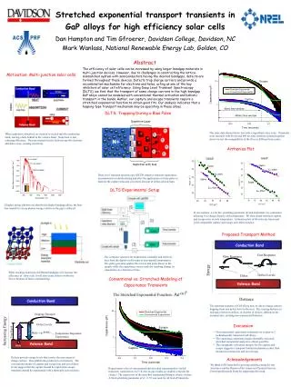
This study focuses on photocapacitance measurements on GaP alloys to understand their suitability for high-efficiency solar cells. The research explores the conduction and valence bands, energy levels, defects, and trap depths in GaP alloys.

E N D
Photocapacitance measurements on GaP alloys forhigh efficiency solar cells Dan Hampton and Tim Gfroerer , Davidson College, Davidson, NC Mark Wanlass, National Renewable Energy Lab, Golden, CO Acknowledgements Davidson Research Initiative American Chemical Society Petroleum Research Fund Jeff Carapella for growing and processing test structures
Conduction Band Conduction Band E=hc/λ Energy + Valence Band Valence Band Valence Band Valence Band
Conduction Band E=hc/λ Energy + Valence Band Valence Band
Conduction Band Conduction Band Conduction Band Conduction Band Energy Electron-Hole Pair + + Valence Band Valence Band
Conduction Band Conduction Band Conduction Band Conduction Band Band Edge Energy + + Valence Band Valence Band
Heat Conduction Band Conduction Band Conduction Band Conduction Band Band Edge Energy Ephoton – Band Gap Energy = Energy Lost + + Valence Band Valence Band
Conduction Band Conduction Band Defect Levels Increasing Energy Trap Depth + + + + + + Valence Band Valence Band Valence Band Valence Band Hole
Conduction Band Conduction Band + Defect Levels Defect Levels Defect Levels + Increasing Energy Capture Trap Depth + + + + + Valence Band Valence Band Valence Band Hole
Conduction Band Conduction Band Defect Levels Defect Levels Defect Levels + Increasing Energy Escape Trap Depth + + + + + + Valence Band Valence Band Valence Band Hole
Picture of Device 1 mm
- - - - - - - - - - - - - - - - - - - - - - - - + - - - - - - - + + + + + + + + + + Photocapacitance N+ P Depletion with bias
- - - - - - - - - - - - - - - - - - - - - - - - + - - - - - - - + + + + + + + + + + Photocapacitance N+ P Depletion without bias
- - - - - - - - - - - - - - - - - - - - - - - - + - - - - - - - + + + + + + + + + + Depletion Layer N+ P Depletion without bias
- - - - - - - - - - - - - - - - - - - - - - - - + - - - - - - - + + + + + + + + + + Depletion Layer T = 77 K N+ P Depletion without bias
- - - - - - - - - - - - - - - - - - - - - - - + - - - - - - - + + + + - + + + + + + Depletion Layer T = 77 K N+ P Depletion without bias
Conclusions • Optical threshold escape energies are higher than thermal threshold energies → Configuration Dependent Traps • GaAsP has a very large trap density, comparable to the density of dopants. This suggests zinc is contributing to the formation of the traps.