The backplane test module
This presentation discusses the Phase One upgrade of the Level-1 Calorimeter Trigger at Mainz University, focusing on the current system's capabilities and the necessary improvements to the trigger algorithm in light of increased luminosity and interaction rates from the LHC. Key topics include the data path from JEM/CPM to CMM, the design of the backplane test module, bandwidth considerations, bit error rate testing, and additional circuitry details. The upgrade aims to maintain high acceptance rates while improving selectivity and data management in a more demanding operational environment.


The backplane test module
E N D
Presentation Transcript
Overview/motivation • Upgrade phaseone and the currentsystem • JEM/CPM-to-CMMdatapath • The Backplane test module • Considerations and requirements • A fewtechnicaldetails and BERT setup • Somewords on the additional circuitry • Outlook The backplane test module Christian Schröder Mainz University Level-1 CalorimeterTrigger Joint Meeting November 5th, 2008
Upgrade phaseoneWhat will happen in phaseone? LHC/beam: Trigger: Level-1 trigger rate can‘tincrease (output rate still < 100 kHz) Have to bemoreselective Acceptanceshould still be as high as possible Simplyraisingthethresholdsis no solution! (pile-upeffects?) • Luminosity will increaseby a factor of two: from 1034 cm-2 s-1 to 2.3·1034cm-2 s-1 • Interaction rate will approximately double • Number of events per bunchcrossing will increasefromabout 20 to about 40 • have to improvethetriggeralgorithm • Buthow and where?
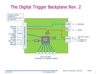
Overview of thecurrent level-1 calorimetertriggersystem • 4 crates à 14 CPMs + 2CMMs: • carry out the e/γ and τ algorithm(Δφ x Δη = 0.1 x 0.1) • 16 thresholds (8 for e/γ and 8 for e/γ/τ) and 16 RoIs per module • 25 links to each CMM @ 40 MHz At that point wehaveonlyinformation of multiplicities and no topologicalinformation. • 2 crates à 16 JEMs + 2 CMMs: • Carry out jet and sumalgorithm (Δφ x Δη = 0.2 x 0.2) • 8 thresholds and 8 RoIs per module • 25 links to each CMM @ 40 MHz
What additional datacouldweuse? • MaybetheRoIs • 8 RoIs per JEM, 2 locationbits per RoI, 8 threshholdbits per RoI • 8 x (2 + 8) bits = 80 bitsfortheRoIs per JEM • Maybe ET, Ex and Eywithfull 12 bitprecision (and notthescaled 6 bit) • 3 x 12 bits = 36 bits per fortheenergy sums per JEM • Total data per JEM: • 80 + 36 bits= 116 bitshave to besent per JEM each 25 ns With 50 links on the backplane to theCMMs data rate needed: 4 x 40 Mbps = 160 Mbps 12bit to 8bit scaling Need to understand wich dataisuseful(Monte-Carlo simulations?)
Bandwidth on the backplane Each CPM or JEM is sourcing a total of 50 lines into two mergers total capacity per module into both mergers is : 50 bit @ 40 Mb/s (25 bit of jet data) 100 bit @ 80 Mb/s (75 bit of jet data) * 200 bit @ 160 Mb/s (175 bit of jet data) * 400 bit @ 320 Mb/s (375 bit of jet data) * * On the JEMs, if we do not need to increase energy sum data volume, any increase on both backplane links can be used for jet data, if the increase in latency on the jet-to-sum processor path is acceptable (requires re-work of current jet processor DAQ interface)
backplane signals Seriesterminated: Scopeshots of JEM signalsoverthelongest backplane trackswithnoise on CMM and VME lines: Parallel terminated: 160 Mbits, CMOS 2.5V 320 Mbits, CMOS 2.5V • For rates ≥ 160 Mbitsweneedtermination at the sink
Rate tests • The rate limit on the backplane is about 160-320 Mb/s on JEMs • We need to understand what the required bandwidth will be on CP and JEP • Understand which data we want to use • We will need to do bit error rate tests on backplane data with a module able to • terminate the signals for data rates ≥ 160Mb/s • deskew each signal line individually • Not possiblewithcurrentCMMs • Build backplane tester based on recent FPGA family providing both termination and deskew
General considerationsforthe backplane test module • datafrom JEMs/CPMs: 400 lines (at themoment 2.5V CMOS, sourceterminated) • Parallel termination at the sink isrequired • externalto ½ VCCO • internalby DCI • 1.5 V CMOS shouldbepossibleas well • variable VCCO • Regional clocks for source synchronous transmission (clock forwarding) • fine tunable per pindeskew • VME––bus(3.3 V, about 49 lines) • TTC clock jittercleaner • PCB iscomparatively expensive • useit also totestsomehigh-speedoptical links • high-speed links upto 6.25 Gbps • SNAP12 upto 75 Gbpseach • route theremaining parallel links on a headerforgeneralusage Xilinx Virtex-5 FX70T FPGA
Schematicoverview Backplane Reduced VME CPLD VME buffer JTAG buffer JTAG header VME 40MHz clock JTAG chain config CF-card Full VME-- System ACE from CPM/JEM FPGA 400 Additional circuitry (opto) Ring ofdiscreteterminators Parrallel links TTC signal High-speed links Clockmuxandfanout 16 pairs Recoveredclock Cleaned clock config Power converters 160 MHz crystalclock JitterCleaner SPI flashmemory
Power dissipation Externalterminationat sink DCI-/internal-terminationat sink VCCO = 2.5 V R = 60 Ohm • VTT = ½ VCCO = 1.25 V • Z0 = 60 Ohm • P = (½ VCCO)2 / Z0 ≈ 26 mW • Ptotal = 400 * 26 mW ≈ 10.4 W a lot of power dissipation (challengingforcooling) changingthesignalstandard to 1.5 V CMOS, i.e. VCCO = 1.5 V • Ptotal = 400 * 9 mW = ~ 3.8 W But: onlypossibleforthe JEMs not forthe CPMs
Overview of the BERT setup Backplane Eachmodule: 1 forwardedclock 24 datalines 1.5V-2.5V CMOS 40-320Mbits • JEMs/CPMscanbemixed (butinbetween has to beoneslotleftempty) • theJEMs/CPMssimplygenerate a test pattern • data (test pattern) issentoverthe backplane • 1 link out of 25 isusedforclockforwarding • the backplane test modulereceives and comparesthedata to expectedpatter • thebiterrorsarecalculated and an errorcountercanberead out via VME • Phase correction of clock and datalines also via VME CPU CPU Backplane Tester JEM JEM/CPM JEM/CPM JEM/CPM JEM/CPM JEM/CPM JEM/CPM JEM/CPM JEM/CPM JEM/CPM JEM/CPM JEM/CPM JEM/CPM JEM/CPM JEM/CPM JEM Backplane Tester TCM
Somewords on the additional circuitry we‘dlike to test someoptical links: • Snap12 optical link module: • upto 75 Gbps (12 x 6.25 Gbps) • up to 300 m lengthover OM3 ribbonfiber • board-edgeormid-boardmounted • low power consumption: ~ 2.5 W TX, ~ 1 W RX per channel • 850nm VCSEL laserarray, MTP/MTO opticalconnector • electrical interface: 12 x 6.25 Gbps CML (compatible with Xilinx GTXs Transceiver) • Rocket I/O GTX Transceiver • cheaplyavailable in manyXilinx Virtex-5 FPGAs • upto 6.5 Gbps per link • up to 48 Transceiver per FPGA (16 in FX70T) • Requires a low-jitterclock
High speeddatapath and clockpath FPGA inputsignals inputs 6.25 Gbps GTX GTX logic/ patterngenerator GTX data GTX GTX TTC signal Snap12 (RX) GTX GTX 12 x 6.25 Gbpselectrical 12 x 6.25 Gbpsoptical GTX Jitter Cleaner Clockrecovery clock GTX GTX GTX GTX lowjitterclock
High speedclock and datapath FPGA inputsignals inputs 6.25 Gbps GTX GTX logic/ patterngenerator GTX data GTX GTX TTC signal Snap12 (RX) GTX • Peak-peakjitter: ~ 7 ps • RMS jitter: ~ 700 fs • Phase drift 50°C – 80°C: < 50 ps • Shouldbesufficientfor 6.5 Gbps GTX 12 x 6.25 Gbpselectrical 12 x 6.25 Gbpsoptical GTX Jitter Cleaner Clockrecovery clock GTX GTX GTX GTX lowjitterclock
Outlook • Wehavealreadystarted • FPGA will bedelivered in about 5 weeks • PCB layout will befinished in about5weeks • Firmware will beprogrammed in parallel • maybetheboard will befullyassembled in about 2 months thenwe‘llbereadyforfirsttests
Total datarates: • 14 CPMs/16 JEMs per crate • CPMs/JEMs aremergedtoleftandright CMM • 24 + 24 datachanels (+ 2 forwardedclocks) per CPM/JEM • 160 Mhz(4x): • 3.84 Gbpstoeach CMM per JEM • 61.44 Gbpstoeach CMM altogether • total datatransfered: • 122.88 Gbps • 240 Mhz(6x): • 5.76 Gbpstoeach CMM per JEM • 92.16 Gbpstoeach CMM altogether • total datatransfered: • 184.32 Gbps • 320 Mhz(8x): • 7.68 Gbpstoeach CMM per JEM • 122.88 Gbpstoeach CMM altogether • total datatransfered: • 245.76 Gbps