Download
1 / 27
331 likes | 517 Views
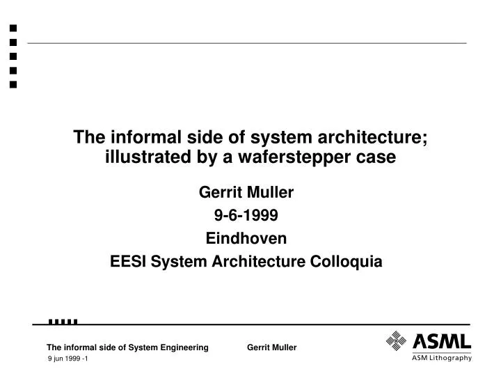
The informal side of system architecture; illustrated by a waferstepper case. Gerrit Muller 9-6-1999 Eindhoven EESI System Architecture Colloquia. The Market. 1997. 2002. semiconductor sales by end-user market. GDP. 33.4 T$. 39.4 T$. 3%. 3%. non PC computing. consumer

E N D
The informal side of system architecture;illustrated by a waferstepper case Gerrit Muller 9-6-1999 Eindhoven EESI System Architecture Colloquia
The Market 1997 2002 semiconductor sales by end-user market GDP 33.4 T$ 39.4 T$ 3% 3% non PC computing consumer electronics communications other applications electronic sales 902.4G$ 1284.2G$ PC’s 32% 16% 17% 18% 17% 17% 26% semiconductor sales other semiconductors IC’s memory 151.7G$ 330.6G$ 15% 13% Equipment sales 22.3G$ 42.8G$ equipment 16% 17% steppers Steppers 3.6G$ 7.3G$ ASML sales 1997: 1.8 Gfl net income: 0.3 Gfl source: Dataquest, ING Barings research www.asml.com
Market fluctuations The semiconductor equipment market shows large fluctuations. 1995 1996 1997 1998 units 177 205 211 162 net sales Mfl 918 1331 1803 1717 net profit Mfl 131 218 329 137 Logistic and manufacturing flexibility is a must.
Cost structure flexibility $ Income Costs margin Market fluctuation Sales
What is a waferstepper? Lightsource Mask (Reticle) Lens Die Wafer
Step & Scan technology reticle Scanning fieldsize Slit Stepping fieldsize Lens Lens wafer 250 mm/s
Main specifications Productivity Imaging Overlay AA (single machine) 40 nm BC (matched) 60 nm 96 Wafers per hour linewidth: 180 nm (1999) critical dimension control For comparison: Wafer diameter 200 mm Die size ca.: 20*20 mm2
Moore’s law (or challenge?) SIA 97 98 99 00 01 02 03 04 05 06 1994 roadmap 250 180 130 1997 roadmap 250 180 150 130 1998 revision 250 180 150 125 1999 proposal 250 180 130 90 leading edge customers 250 180 130 100 linewidth in nm.
Product roadmap ATHENA/TIS 2 kHz laser Quadrupole T1100 193 nm scanner Atlas 300 mm body S400 I-line scanner T400 I-line scanner S700 DUV scanner T700 DUV scanner /900 193 nm scanner 5500 scanner body /400 i-line scanner /500 DUV scanner /700 DUV scanner /300C DUV stepper /300D 5500 stepper body /250C i-line stepper
Modular subsystems illuminator light source reticle handling reticle stage measurement lens UI console contamination and temperature control electronics cabinets wafer handling wafer stage base frame
System engineering imaging overlay productivity mechanics optics control measurement contamination & temperature
System Engineering Integral system design leading in system- consistency integrity balance specification decomposition modularization verification supporting system- integration risk reduction Product and Competence definition synergy of products and programs roadmap vision
Profile of the system engineer • Highly skilled: • Communication • Teamwork • Documentation • Multi-tasking (many parallel activities, • many interrupts) • Conceptual • Pragmatic; • balance between conceptual and pragmatic • Insight in process • (Who does What, When for Whom) • Insight in Politics • Authority by expertise • Flexible and open, egoless • Ability to absorb new know how fast, curiosity • Constructive Critical (inward and outward) • Generalist, know how areas: • Source, illumination • Projection • Dynamic performance • Alignment • Metrology • C&T • Wafer+reticle handling+interfacing • Aerial imaging • Imaging, processing, application • throughput • Safety • Reliability, uptime, robustness • Testability • fab interfacing; HW+SW infrastructure • configuration management • Software architecure • Electronics architecture • Mechanical architecture
Understanding the context of the system Resists Fab logistics devices Fab automation Semiconductor design SPC Processing Tracks Wafer Reticle production Yield optimization Metrology Waferstepper Reticles Reticle logistics Matching Operator Wafer logistics Fab layout Contamination maintenance Inspection and monitoring utilization Fab cost model Fab infrastructure
Understanding the business context • Other players: • equipments vendors • system integrators • lease companies • fab designers • consultants • mask makers • resist makers • wafer makers • OEM’s: laser • intimate partners: lens Yield Value of performance (MHz) CD control Parameter trade-offs • Business models of the customer: • design houses • foundries • vertical integration Limited number of customers; Many systems per customer
Understanding the people context informal relations profesionalism facilitation maturity people strategy Style technologies Skills Shared Value family, home situation People roles, tasks Organization Well-being motivation teams Process Culture incentives location maturity company projects principles reviews
Technology context Temperature sensitivity UV sensitivity Transmission Reflection Stiffness modes coatings Motors Construction materials Optical Materials uniformity Construction Lens Actuators Servo’s bandwidth Gratings Air showers Lasers C&T frequency Mechanics Dynamics Imaging Optics Cooling Pulse timing Lamps Robotics Lithography Vacuum clamping energy Dose control Interferometers Measurement Dose sensor Mirrors Measurements gratings home sensors Light sensors SW control Measurement lasers Pre- amplifiers Capacitive sensors Analog signal procesing Digital signal processing Hall sensors Digital infrastructure Real time executives
Project Context SPS/SDS ATP FAT/SAT Quality assurance Customers Slot list Beta test Alfa test Production space Project definition Project documentation Functional models prototypes Production engineers production Critical path Verification Specification Training milestones Installation Plan Manuals Budget Time review Progress Support Service engineers tracking Long lead items Material planning Risks Development resources Spare parts TPD Baby sitters costs Scenario’s Critical resources activities outsourcing
Making specification and design choices Technology Competence manager System Design System context Overview Common sense proposals 80/20 optimization, balance knowledge risks authority marketing, application manager System Engineer(s) Business context Business manager People context line manager • design for: • market • verification • manufacturability • serviceability • etcetera • architecture for: • control • dynamics • optics • mechanics • etcetera Project context Product Development manager
Overlay budget Off axis pos meas accuracy 4 nm Off axis Sensor repro 3 nm Global alignment accuracy 6 nm Stage Al. pos. meas. accuracy 4 nm Blue align sensor repro 3 nm Lens Matching 25 nm Reticle 15 nm System adjustment accuracy 2 nm tracking error WS 2 nm tracking error X, Y 2.5 nm Process Overlay 80 nm Matched Machine 60 nm Single Machine 30 nm Stage overlay 12 nm Position accuracy 7 nm tracking error RS 1 nm tracking error phi 75 nrad Stage grid accuracy 5 nm alignment repro 5 nm Matching Accuracy 5 nm Frame stability 2.5 nm Process dependency sensor 5 nm Metrology stability 6 nm Interferometer stability 1 nm
Development phases 0 1 2 3 4 feasibility definition system design subsystem spec subsystem design engineering integration verification field monitoring business impact prs sps sds tps alfa test TAR beta test TAR plan cost, effort,time integration plan eps eds tps prototype tpd
SPS contents checklist 0 1 2 3 feasibility definition system design subsystem spec subsystem design engineering overview doc tree, structure product lifecycle option structure draft option structure • performance requirements • imaging • overlay • throughput • functional requirements • functional model (extern) • factory integration • user interface • functional requirements draft • functional model (extern) draft • operations requirements • serviceability • manufacturability • operations requirements draft • serviceability • manufacturability • environment requirements • wafer, reticles • power, gases, water, etc. • weight size • transport • machine requirements • design constraints, f.i. robustness • safety • reliability • COG, COO • interoperability
reliability/uptime budget reliability/uptime budget draft SDS contents checklist 0 1 2 3 feasibility definition system design subsystem spec subsystem design engineering doc tree, structure overview draft doc tree, structure draft overview decomposition in subsystems decomposition in subsystems draft performance budgets performance budgets draft functional model (design) functional model (design) draft functional model (design) concept function allocation function allocation draft function allocation concept control architecture control architecture draft SW architecture SW architecture draft Electrical architecture handling interfaces power, gas, water, etc budgets power, gas, water, etc budgets draft mechanical layout budgets mechanical layout budgets draft costprice budget costprice budget draft consumable budget consumable budget draft interoperability design safety analysis safety design diagnostic analysis diagnostic design accessability set up sequence tolerance budget cycle time budget transport design
Definitions PRS Product Requirement Specification What should the product be Marketing SPS System Performance Specification What will the product be SE SDS System Design Specification How will it be made SE TPS Test Performance Specification What and how will it be tested SE TAR Test Acceptance Report Testresult SE EPS Element Performance Specification What D&E EDS Element Design Specification How D&E TPS Test Performance Specification What and how will it be tested D&E TAR Test Acceptance Report Testresult D&E EPS, EDS, TPS are recursively applied from subsystem level to monodisciplinary module level
Concurrent engineering, Integration dynamical performance subsystem1 design subsystem2 design imaging overlay metrology Subsystem n design levelling Concurrent engineering Integration prototypes Final integration
Overlay budget Off axis pos meas accuracy 4 nm Off axis Sensor repro 3 nm Dramatic increase of complexity! 2003: 35 nm Global alignment accuracy 6 nm Stage Al. pos. meas. accuracy 4 nm Blue align sensor repro 3 nm Lens Matching 25 nm Reticle 15 nm System adjustment accuracy 2 nm tracking error WS 2 nm tracking error X, Y 2.5 nm Process Overlay 80 nm Matched Machine 60 nm Single Machine 30 nm Stage overlay 12 nm Position accuracy 7 nm tracking error RS 1 nm tracking error phi 75 nrad Stage grid accuracy 5 nm alignment repro 5 nm Matching Accuracy 5 nm Frame stability 2.5 nm Process dependency sensor 5 nm Metrology stability 6 nm Interferometer stability 1 nm