Download
1 / 58
580 likes | 598 Views
Learn how to choose the ideal amplifier for your CDAC SAR A/D system, covering power supply rails, noise factors, bandwidth, and more. Understand key parameters like LSB size, offset drift, and distortion to optimize performance. Get expert advice from industry leaders for successful amplifier selection.

E N D
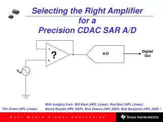
Selecting the Right Amplifier for a Precision CDAC SAR A/D With Insights from:Bill Klein (HPL Linear), Rod Burt (HPL LInear), Bernd Rundel (HPL DAP), Rick Downs (HPL DAP), Bob Benjamin (HPL DAP) Tim Green (HPL Linear)
Power Supply Rails Size of LSB Offset Drift Factors of Concern • Noise • Bandwidth • Distortion • A/D Architecture Target Example: +5V, 16-Bit, 100kHz, CDAC, SAR, A/D Application
Bipolar +/- 15V Implies: +/-10V signals Power Supply Rails • Single Supply • +5V • +3.3V • +1.8V • Signal ranges: +1.5V to +5V
Signal range is critical +/-10V is a 20V range 12 bits: 20V/4,096 = 4.88mV per LSB 16 bits: 20V/65,536 = 305µV per LSB +5V range 12 bits: 5V/4,096 = 1.22mV per LSB 16 bits: 5V/65,536 = 76.2µV per LSB 24 bits: 5V/16,777,216 = 298nV per LSB +3.3V range 12 bits: 3.3V/4,096 = 806µV per LSB 16 bits: 3.3V/65,536 = 50.4µV per LSB 24 bits: 3.3V/16,777,216 = 196nV per LSB LSB Size
If all you have to work with is 38µV (1/2 LSB)… Offset Voltage becomes significant Offset from differential bias current, too! OPA335 as an example Single Supply Input offset less than 20µV Temperature Changes If your system has to operate from -25°C to +75°C, you have a 100°C range of temperature change. If all you have is 38µV (1/2 LSB)… And 20 µV is used up by offset, then you have 18 µV allowed for drift, so you can handle 180nV/°C of drift Note: Offset effect may be compensated in the system software! DC Parameters
Noise - depends upon bandwidth Resistor noise 1K ohm resistor = 579nV @ 25°C, 20kHz bandwidth. Current noise Voltage noise Sampling Noise of A/D > Tens of μVolts Distortion THD+N of a 16-bit converter should be better than -98dB, or 0.0011% - again, over the bandwidth of interest. Suitable op amps: OPA627(Dual Supply) OPA350, OPA134 (Single Supply) Single Supply Op Amps As common mode voltage changes, op amp passes through different regions of bias - this results in something similar to crossover distortion AC Parameters
Single Supply RRI Plot - VOS vs CMV (Most RRI Op Amps Except OPA363/OPA364) OPA2340 (Dual: VOUT1 & VOUT2 from different halves) Gain=X100 Diff Amp Configuration CMV CH1 VOUT1 CH2 CH3 VOUT2
Single Supply RRI Alternate Avoids CM Input “Crossover”
ZIN is RI (typically < 100kΩ) instead of >100MΩ range VOUT of Buffer is Inverted from VIN VCM does not move and is steady at 1/2VCC Mismatch in ratios of RF / RI = 1 and RB1 / RB2 = 1 Gain & Offset Errors RI, RF, RB1, RB2 are additional noise sources Single Supply Inverting “Buffer”
Input Buffer Selection • Charge injection causes large spike which must settle in tSAMP. • Adding a capacitor (and possibly a resistor) can reduce spike • Op amp must be capable of charging capacitance in tSAMP to 0.5LSB. Low output impedance at high frequency required. • OPA627 (Dual Supply), OPA350 (Single Supply)
What Settling Time? • Think of a linear voltage regulator – There are TWO Settling Times. • Line Transient • Load Transient
What Settling Time? • Similar to Linear Regulator Line Transient =Load Transient = Input Step Voltage; Output Step Voltage; Output Voltage Slew Rate Output Step Current
Response to change in input signal Includes Slew Rate. Op Amp data sheets MAY address Settling Time to 0.01% But we need 0.0007629% for a 16 bit system Op Amp “Line Transient”
We know the load is the input capacitance of the A/D (CSH) We do NOT know the starting voltage on CSH. Possible voltages: GND, Mid-Rail, Random The Op Amp data sheet does NOT even mention “Load Transient” response. “Load Transient” is WORST
System Design Variables Op AmpFilterADC Noise, Signal BW, Noise Filtering, Acquisition Time, CMV Range, Slew Rate, Cload Isolation, Architecture (CDAC SAR) Output Impedance, Settling Time, Charge Bucket Power Supply, Load Transient, Gain Error, (Flywheel) Data Rate, Resolution, Power Supply, VOS vs CMV Input, ADC Input, ADC Ref In Circuit Topology, THD + Noise
70% Applications Slow Moving “Real World Process” Signals Fast Acquisition & Conversion Allows More System Time For Processing, Computation, Decision Making Multiplexed, Scanning Systems for Slow Moving Signals 30% Applications AC Fast Moving Dynamic Signals “Real Time” Processing of Input Signals Assume for our analysis that during sample timeVIN is constant SAR A/D < 500kHz
Analysis Will Use • Tricks • Data Sheet Parameters • Factory Only Parameters • Rules of Thumb • Testing
Acquisition Time (tSMPL): The time the internal A/D sample capacitor is connected to the A/D input. Conversion Time (tCONV) The additional time the A/D requires to convert the analog input to a digital output after the acquisition time (tSMPL) is complete. Throughput Rate [Sampling Rate] Maximum frequency at which A/D conversions can be repeated i.e. 100kHz Throughput Rate [Sampling Rate] implies that an input analog signal may be converted every 10μs. A/D Converter Terms
Standard ADS8320 Timing tSMPL= 4.5 Clk Cycles min
A/D tSAMPL Trick 2x tSAMPL= 84% Throughput Rate
“16 Bit, High Speed, 2.7V to +5V, micropower sampling A/D” VCC = +5V, VREF = +5V Throughput Rate (Sampling Rate) = 100kHz DCLOCK = 2.4MHz, tSAMPL=1.88μs Input Signal = 4.87VPP (65mV to +4.935V range),1kHz max SNR = 88dB @ 1kHz THD = -86dB @ 1kHz SINAD = 84dB @1kHz SFDR = 86dB ENOB = 14.33 ADS8320 Application Specs
Application: Single Supply = +5V Buffer – NO CM Input Crossover ! Slew Rate to track 1kHz Input Wideband for good gain flatness: 1kHz, G=1 Wideband for fast transient response to Noise Filter Transients Low Noise for 16 Bit performance Fast Settling time for output transients Adequate Output Drive Current for Filter Transients RRIO for 65mV to +4.935V Input and Output on +5V Supply Best Industry Choice OPA363 or OPA364 (OPA363 with Shutdown feature) “1.8V, 7MHz, 90dB CMRR, Single-Supply, Rail-To-Rail I/O” OP Amp Buffer Application Specs
OPA363/OPA364 Application Specs • SRmin (V/μs) = 2 πfVOP (1e-6) • Minimum Slew Rate to track input sinewave (@<1% Distortion?) • SRmin = 2∙ π∙1kHz∙(4.87Vpp/2)∙(1e-6) = 0.015V/μs • OPA363/OPA364 = 5V/μs • Choose Op Amp SR > 2 X SRmin • Gain Error • AVCL = Aol/(1+Aolβ) • Aol @1kHz = 80dB = 10000 • β = 1 for Unity Gain Follower • AVCL= 10,000/(1+10000∙1) = 0.99990001 • 0.009999% Gain Error @ 1kHz • ≈ 12 Bit (1/2 LSB Accuracy) • Calibrate gain error at system level • Many systems are more concerned about relative changes than absolute • A/D Initial Reference Error (0.02% < Typical Range < 0.2%) • Settling Time • OPA363/OPA364: tS = 1.5μs to 0.01%, VS=+5V, G=+1, 4V Step • A/D tSAMP = 1.88μs so this looks like a possible good candidate • tS to 0.01% < tSAMP
OPA363/OPA364 Application Specs (continued) • THD+Noise • OPA363/OPA364: • THD+N = 0.002%, G=1, RL=2kΩ, VS=5V, f=1kHz, VOUT = 1Vrms • 16Bit desired 0.0011% • Open Loop Output Resistance (RO) • OPA363/OPA364: RO = 200Ω • Output Current • OPA363/OPA364: IO+ = 40mA,VOUT = +/-0.75V, +/-VS = +/-2.5V • OPA363/OPA364: IO- = 40mA,VOUT = +/-0.5V, +/-VS = +/-2.5V • OPA363/OPA364: IO+ & IO-= 10mA,VOUT = +/-2.25V, +/-VS = +/-2.5V
Filter Application Specs • RSW = 100Ω (Not needed for Buffer & Filter Calculations) • CSH = 50pF • Worst case ΔVacross CSH is VREF • VREF = +5V • tSAMPL = 1.88μs
Filter Application Specs (cont) • Charge Transfer Equation: Q = CV • Charge required to charge CSH to VREF • QSH = CSHVREF • QSH = 50pF∙5V = 250pC • IDEAL CFLT (What does CFLT have to be for 1/2 LSB droop on CFLT to change CSH by VREF) • “Charge Bucket” to fill CSH with only a 38μV (1/2LSB) droop on CFLT • QFLT =QSH • QFLT = CFLT (38μV) • 250pC = CFLT (38μV) → CFLT = 6.6μF • IDEAL CFLT = 6.6μF • Not a good, small, cheap high frequency ceramic capacitor • Not practical for Op Amp to drive directly (stability, transient current) • Isolation resistor likely not large enough to help isolate Cload and still meet necessary filter time constant
Filter Application Specs (cont) • Partition the “Charge Bucket” • 95% from CFLT • 5% from Op Amp • CFLT value required to provide QSH with <5% droop on CFLT • QFLT = QSH • QFLT = CFLT (0.05VREF) • 250pC = CFLT (0.05∙5V) → CFLT = 1nF • During tSAMPL the Op Amp must replace 5% VREF on CFLT • Ensure CFLT is at least 10X > CSH • This implies dominant load for Op Amp Buffer is CFLT • 1nF = 20 X 50pF CFLT = 20X CSH
Filter Application Specs (cont) • Time required for CSH & RSW to settle to 1/2LSB @ 16 Bits • RSW = 100Ω (If unknown assume 100 Ω) • τA/D = RSW CSH = 100Ω∙50pF = 5ns • tA/D settle = 12 τA/D = 60ns • Small in comparison to tSAMPL • RFLT Calculation • tFLT settle = tSAMPL= 12τFLT • tFLT settle = 1.88μs = 12τFLT • 12τFLT = 1.88μs→ τFLT = 157ns • τFLT* = 0.60 τFLT • 40% Margin for: • Op Amp Output Load Transient • Op Amp Output Small Signal Settling Time • τFLT* = RFLT CFLT • 0.60∙157ns= RFLT 1nF → RFLT =94.2Ω • Use RFLT = 100Ω
Op Amp Transient Output Drive to RFLT &CFLT IOpk max = (5% VREF)/(RFLT) = 250mV/100Ω = 2.5mA OPA363/OPA364: IO+ & IO- = 2.5mA,VOUT ≈ +/-2.428V, +/-VS = +/-2.5V VS = +5V Single Supply VOUT = +4.928V Filter Application Specs (cont)
Op Amp + Filter Analysis – Small Signal • Modified Aol due to RFLT & CFLT • fPX = 1/[(RO + RFLT)CFLT2π] • fPX = 1/[(200Ω + 100Ω)1nF∙2π] = 530kHz • fZX = 1/[RFLTCFLT2π] • fZX = 1/[100Ω∙1nF∙2π] = 1.6MHz • Stability Check • At fcl = 3.2MHz “Rate-of-closure” is 20dB/decade fZX cancels fPX before fcl • fPX and fZX are < decade apart • Phase of pole will be cancelled by phase of zero • Buffer Closed Loop Gain Bandwidth • fcl = 3.2MHz • VOA BW >2x fcl • VOA f-3db = fcl = 3.2MHz • VOA BW > 2*fcl = 2*3.2MHz = 6.4MHz • OPA364 BW = 7MHz
Log Scale Trick Log Scale Trick (fP = ?): 1) Given: L = 1cm; D = 2cm 2) L/D = Log10(fP) 3)fP = Log10-1(L/D) = 10(L/D) 4) fP = 10(L/D) = 10(1cm/2cm) = 3.16 5) Adjust for the decade range working within – 10Hz-100Hz decade fP = 31.6Hz 6) L = Log10(fp’)X D where fp’ = fp normalized to the 1-10 decade range – fP = 31.6 fP’ = 3.16
OP Amp + Filter Analysis – Small Signal (cont) Small Signal Transient Response • Small Signal Rise Time (10% to 90%) • tr = 0.35 / fcl • tr = 0.35 / 3.2MHz = 0.109µs = 109ns • Small Signal Settling Time Constant • τsettle ss = 1/(2πfcl) • τsettle SS = 1/(2π∙3.2MHz) = 49.7ns • Small Signal Settling Time • tsettle ss = 12τ = (12)(49.7ns) = 596.4ns • Small Signal Transient Response < 40% tSAMPL • ttran ss< 40 % tSAMPL • tr + tsettle SS< (0.40)(tSAMPL) • 109ns + 596.4ns < (0.40)(1.8µs) • 705.4ns ? < 720ns • Close enough to proceed
OP AMP + Filter Noise Analysis • Op Amp + Filter • BW = 1.6MHz • Vnoise = (Op Amp Noise)[(Filter BW)(Single Pole Noise BW Ratio)] • Vnoise = [17nV/√Hz][√(1.6MHz∙1.57)] = 26.94μVrms • White Noise Dominant with 1.6MHz BW • Resistor Noise = √(4KTRB) • B = (Filter BW)(Single Pole Noise BW Ratio) = 1.6MHz∙1.57 = 2.5MHz • KT = 4.11x10⁻²¹ @ 25°C • 100Ω noise = √[4(4.11x10⁻²¹)(100 Ω)(2.5MHz)] = 2.03μVrms → Negligible • A/D Noise • SNR A/D = 88dB • SNR A/D = 20 Log10 (VINrms/Vnoiserms) • VIN = 5VPP = 1.7675Vrms • A/D Vnoise = 70.365μVrms • System SNR • SNR System = 20Log10 {[VINrms] / √[(ADC Vnoise)2 + (Vnoise)2]} • SNR System = 20Log10 {[(4.87Vpp/2)(0.707)] / √[(70.365 μVrms)2 + (26.94μVrms)2]} • SNR System = 87.18dB • ENOB (ideal) = [SNR(dB) – 1.76] / 6.02 • ENOB System = [87.18 -1.76] / 6.02 = 14.19
ADS8320 On Test System ADS8320 Data Sheet: SNR = 88dB THD = -86dB SINAD = 84dB SFDR = 86dB ENOB = 14.33
OPA364, Filter, ADS8320 On Test System Op Amp+Filter+ADS8320 Calculated: SNR = 87.18dB ENOB = 14.19
Comparison of Tests ADS8320 Only OPA364, Filter, ADS8320 AD8S320 Data Sheet: SNR = 88dB THD = -86dB SINAD = 84 DB SFDR = 86dB ENOB = 14.33 Op Amp+Filter+ADS8320 Calculated: SNR = 87.18dB ENOB = 14.19
Reference is DC, right? So a slow op amp is OK? No! Same thing happens on reference input as analog input, but it must settle in 1 clock cycle! Requirements on reference buffer are even more stringent. Possible Circuit: Reference Buffer Selection
Promise of more to come… • This is just the beginning • Tuning for BEST results • Filter Capacitor • AC Magnitude • DC Offset • Sample Rate • Different converters • Testing DC parameters • Testing AC parameters • Rules of Thumb & Tricks • To Optimize Op Amp, Filter, A/D System • Each Customer WILL NEED TO TEST His/Her Final Application
Selecting the Right Amplifier for a Precision CDAC SAR A/D Summary of Procedure
Buffer / Filter Selection for CDAC SAR A/D Input • Specify System Voltages • Define maximum input signal • Highest Frequency • Largest Voltage Swing • Choose A/D Converter • Select Number of Bits of Resolution • Select Maximum Throughput Rate (Sampling Rate) • Select Minimum Acquisition Time (tSAMP) • Use DCLOCK stop trick if longer tSAMP is desired • Choose CFILT • VREF is max ΔV across CSH • QSH = CSHVREF • QFLT = QSH • QFLT = CFLT(0.05VREF) • Ensure CFLT is at least 10X > CSH
Buffer / Filter Selection for CDAC SAR A/D Input (cont.) • Choose RFILT • tFLT settle = tSAMPL = (#τ)τFLT (where #τ is number of time constants to reach 1/2LSB settle – i.e. 12 time constants for settling to ½ LSB for 16Bit A/D) • Solve for TFLT • τFLT* = 0.60 τFLT • τFLT* = RFLT CFLT Solve for RFLT • Calculate Op Amp Transient Output Drive to RFLT &CFLT • IOpk max = (5% VREF)/(RFLT) • Calculate Op Amp Unity Gain Bandwidth • First pass select unloaded Op Amp UGBW > 2 X VFLT f-3db • VFLT f-3db = 1/[RFLTCFLT2π]
Buffer / Filter Selection for CDAC SAR A/D Input (cont.) • Op Amp Selection - General • Choose Buffer or Inverting Buffer Configuration • If Buffer on Single Supply beware of “Input CMV Crossover” • Slew Rate: SRmin (V/μs) = 2πfVOP (1e-6) • Choose Op Amp SR > 2 X SRmin • Gain Error (at the maximum input signal frequency) • AVCL = Aol/(1+Aolβ) • A/D Initial Reference Error (0.02% < Typical Range < 0.2%) • Settling Time • tS to 0.01% < tSAMP • THD+N • Close to desired ½ LSB chosen Accuracy • Op Amp Current Drive [IOpk max = (5% VREF)/(RFLT)] • Choose for VOPK @ IOpk max • Unity Gain BW: • First pass select unloaded Op Amp BW > 4 X VFLT f-3db • Output Resistance (RO) • Factory Only Parameter (if not specified in data sheet)
Buffer / Filter Selection for CDAC SAR A/D Input (cont.) • Op Amp Selection – Small Signal • Modify Aol due to RFLT & CFLT • fPX = 1/[(RO + RFLT)CFLT2π] • fZX = 1/[RFLTCFLT2π] • Stability Check • At fcl = 3.2MHz “Rate-of-closure” is 20dB/decade fZX cancels fPX before fcl • fPX and fZX are < decade apart Phase of pole will be cancelled by phase of zero • Buffer Closed Loop Gain Bandwidth = fcl (from modified Aol) • VOA BW >2x VFLT BW • VOA f-3db = fcl • VFLT f-3db = 1/[RFLTCFLT2π] • Small Signal Transient Response • ttran ss< 40 % tSAMPL • tr + tsettle SS< (0.40)(tSAMPL) • τsettle ss = 1/(2πfcl) • tsettle ss = (#τ) X τsettle SS
Buffer / Filter Selection for CDAC SAR A/D Input (cont.) • Op Amp + Filter Noise • Vnoise = (Op Amp Noise)[(Filter BW)(Single Pole Noise BW Ratio) • Single Pole Noise BW Ratio = 1.57 • White Noise Dominant at wide BW • Resistor Noise = √(4KTRB) • B = (Filter BW)(Single Pole Noise BW Ratio) Negligible? • KT = 4.11x10⁻²¹ @ 25°C • A/D Noise • SNR A/D = 20 Log10 (VINrms/Vnoiserms) • Calculate A/D Vnoise • System SNR • SNR System = 20Log10 {[VINrms] / √[(ADC Vnoise)2 + (Vnoise)2]} • Calculate SNR System 13)System ENOB = [SNR(dB) – 1.76] / 6.02 • Calculate System ENOB • Prototype & Test Final Configuration
An Analysis of an Op Amp’s Open Loop Output Resistance and Closed Loop Output Resistance Appendix - Facts about RO and ROUT