Download
1 / 31
310 likes | 407 Views
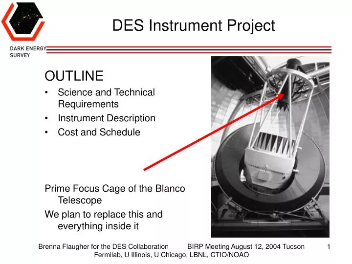
DES Instrument Project. OUTLINE Science and Technical Requirements Instrument Description Cost and Schedule Prime Focus Cage of the Blanco Telescope We plan to replace this and everything inside it. Science and Technical Requirements.

E N D
DES Instrument Project OUTLINE • Science and Technical Requirements • Instrument Description • Cost and Schedule Prime Focus Cage of the Blanco Telescope We plan to replace this and everything inside it Brenna Flaugher for the DES Collaboration BIRP Meeting August 12, 2004 Tucson Fermilab, U Illinois, U Chicago, LBNL, CTIO/NOAO
Science and Technical Requirements TheScience Requirementsflow toTechnical Requirements • 5000 sq-deg in the South Galactic Cap in 30% of 5 years • Galaxy cluster catalogs • Complete, simple selection function to z=1, • photometric redshifts to z=1.3 with dz < 0.02. • A small and stable PSF • Seeing < 1.1” FWHM with median < 0.9'' FWHM • PSF stable to 0.1% over a 1 sq-cm (9 sq-arcmin) area • 3 sq-degree camera with ≥ 2.2 deg FOV • SDSS g,r,i,z filters covering 400 to 1100nm • Limiting mag of griz =22.8, 23.4, 24.0, 23.6 • QE > 50% in the z band • Photometric calibration to 2%, goal to 1% • Read noise <10 e- • Pixel size <0.3” /pixel • < 0.4” FWHM in the i and z bands Brenna Flaugher for the DES Collaboration BIRP Meeting August 12, 2004 Tucson Fermilab, U Illinois, U Chicago, LBNL, CTIO/NOAO
DES Instrument Reference Design Instrument Construction Organization 1.2.1 CCDs 1.2.2 CCD Packaging 1.2.3 Front End Electronics 1.2.4 CCD Testing 1.2.5 Data Aquisition 1.2.6 Camera Vessel 1.2.7 Cooling 1.2.8 Optics 1.2.9 Prime Focus Cage 1.2.10 Auxiliary Components 1.2.11 Assembly and Testing 3556 mm Camera Scroll Shutter 1575 mm Filters The Reference Design represents our current design choices and may change with more analysis Optical Lenses Brenna Flaugher for the DES Collaboration BIRP Meeting August 12, 2004 Tucson Fermilab, U Illinois, U Chicago, LBNL, CTIO/NOAO
Optics Design Corrector • 2.2 deg. FOV Corrector • 5 powered elements (Fused Silica) • one aspheric surface (C4) • four filters – griz needed for DES • others can be used • More details of the design in the next talk (Steve Kent) • Cost for the glass ~ 660k$ • Cost for figuring ~ $1M • ~ 1.5 yr delivery Brenna Flaugher for the DES Collaboration BIRP Meeting August 12, 2004 Tucson Fermilab, U Illinois, U Chicago, LBNL, CTIO/NOAO
CCDs • Reference Design: LBNL CCDs • QE> 50% at 1000 nm • 2k x 4k • 15 micron pixels • 250 microns thick • fully depleted (high resistivity) • back illuminated • 4 side buttable • readout 250 kpix/sec • 2 RO channels/device • readout time ~17sec • fringing eliminated • PSF controlled by bias voltage R&D on LBNL CCDs nearly finished. LBNL CCDs have been used at LICK and on the WIYN Telescope and on the Mayall Brenna Flaugher for the DES Collaboration BIRP Meeting August 12, 2004 Tucson Fermilab, U Illinois, U Chicago, LBNL, CTIO/NOAO
CCD QE and Read noise To get redshifts of ~1 we spend ~50% of survey time in z-band. LBNL CCDs are much more efficient in the z band than the current devices in Mosaic II Read noise for a recently finished DALSA 2k x 4k 250 kHz → 7e- Brenna Flaugher for the DES Collaboration BIRP Meeting August 12, 2004 Tucson Fermilab, U Illinois, U Chicago, LBNL, CTIO/NOAO
CCD Acquisition Model Reference Design Acquisition Model • Order CCDs through LBNL – good relationship with commercial foundry • Foundry delivers wafers to LBNL (~650 microns thick) • LBNL • applies backside coatings for back illuminated operation • oversees thinning (~ 250 microns thick) and dicing • tests all devices on cold probe station • LBNL delivers all tested, unpackaged devices to FNAL • FNAL packages and tests CCDs • Prepared to package ~ 160 CCDs (spares, yield) • CCD Wafers: • Existing masks have 2/wafer • to be cost efficient we will make new masks with 4/wafer Brenna Flaugher for the DES Collaboration BIRP Meeting August 12, 2004 Tucson Fermilab, U Illinois, U Chicago, LBNL, CTIO/NOAO
Packaging • CCD Packaging will be done at Fermilab • LICK and LBNL have already successfully packaged small quantities. • We are developing a working relationship with R. Stover at LICK (we visited in July) to learn packaging techniques Invar Foot CCD packaged at LBNL AlN circuit board Wirebonds to CCD CCD Packaging is very similar to building the components of silicon vertex detectors. Fermilab has built many vertex detectors for CDF and D0, and is contributing to CMS Brenna Flaugher for the DES Collaboration BIRP Meeting August 12, 2004 Tucson Fermilab, U Illinois, U Chicago, LBNL, CTIO/NOAO
Packaging and Testing Process • Packaging and testing keep up with anticipated CCD delivery rate of 20/month (5 wafers). • Packaging: • one CCD takes ~ 1 week to complete • Plan to have capabilities to start 2/day • Testing: • estimate 2 days/CCD • 3 identical test stands needed to keep up with 5 CCDs/week • LBNL cold probe test results will guide which CCDs to package 1st • Assume 60 good devices from production run and up to 18 good devices from preproduction run Brenna Flaugher for the DES Collaboration BIRP Meeting August 12, 2004 Tucson Fermilab, U Illinois, U Chicago, LBNL, CTIO/NOAO
CCD Test Stand and Acceptance Criteria • Testing • linearity, full well depth, QE, CTE, readnoise, dark current • Testing and acceptance criteria will be defined as we gain experience with LBNL CCDs • Will also consider impact of acceptance criteria on community • Multiple tilings reduces impact of bad regions • Study with 100 consecutive bad columns found ~1.5% of tiling area was imaged less than 3 times after 5 complete tilings Brenna Flaugher for the DES Collaboration BIRP Meeting August 12, 2004 Tucson Fermilab, U Illinois, U Chicago, LBNL, CTIO/NOAO
Camera Reference Design Focal Plane Camera Design feed through board 62 2k x 4k CCDs for main image, 4-side buttable, 15 micron pixels 8 1k x 1k CCDs for guiding and focus Frontend electronics Focal Plane Brenna Flaugher for the DES Collaboration BIRP Meeting August 12, 2004 Tucson Fermilab, U Illinois, U Chicago, LBNL, CTIO/NOAO
Camera Vessel Cooling/ Vacuum spool piece Camera is separated into two spool pieces: one for signal feed throughs one for cooling and vacuum services Removal of cooling spool piece allows access to back of focal plane and cables • Vacuum feed through board brings signals out of cryostat Brenna Flaugher for the DES Collaboration BIRP Meeting August 12, 2004 Tucson Fermilab, U Illinois, U Chicago, LBNL, CTIO/NOAO
Cooling and Integration • Reference Design has LN2 reservoir inside cryostat • Fill from recondensing dewars on floor • investigating alternative: Gifford-McMahon cryo coolers on cooling spool piece which condense N2 directly into reservoir Will fully assemble prime focus cage at FNAL and test all systems together (corrector, focal plane, cooling, data acquisition, data management....) before shipping to Chile Brenna Flaugher for the DES Collaboration BIRP Meeting August 12, 2004 Tucson Fermilab, U Illinois, U Chicago, LBNL, CTIO/NOAO
Front End Electronics and DAQ • Large focal plane implies long cables between CCD and electronics crates • Reference design has clock drivers and preamps as part of the cable assembly • Goals are noise < 5 e-, linearity <0.25%, support a readout rate of 250 kpix/sec • Reliable operation requires careful consideration of internal and external components • Minimize heat generated in the PF cage by locating DAQ off telescope off the cage Brenna Flaugher for the DES Collaboration BIRP Meeting August 12, 2004 Tucson Fermilab, U Illinois, U Chicago, LBNL, CTIO/NOAO
DAQ Parameters Image CCDs Guide CCDs # CCDs 62 (+4) 4 2k x 4k (1k x 1k) 1k x 1k Pixels/CCD 2 2 Amps/CCD Digitization rate 250 kHz (17 s) 1 MHz (0.5 s) 971 MB 8 MB Bytes/image Data rate 57 MB/s 16 MB/s FEDAQ Data Acquisition DES data rates are relatively high by astronomy standards, but not for particle physics. • We will use the Monsoon data acquisition system, developed by NOAO. • We will modify it to separate digital and analog functionality. Using Monsoon shortens development time and enables collaboration with NOAO and other Monsoon users. Brenna Flaugher for the DES Collaboration BIRP Meeting August 12, 2004 Tucson Fermilab, U Illinois, U Chicago, LBNL, CTIO/NOAO
We will modify this part. Data Acquisition Monsoon architecture: DES Modifications: ADCs will reside on the telescope.The rest of the electronics will be off the telescope. • Save space and power on the telescope. • Reduce noise (ADCs are closer to the CCDs). • Save money. Brenna Flaugher for the DES Collaboration BIRP Meeting August 12, 2004 Tucson Fermilab, U Illinois, U Chicago, LBNL, CTIO/NOAO
We Can Do This! The DES collaboration has assembled a team of experienced scientists, engineers, designers and technicians The Silicon facility at Fermilab has experience building the Run 0, I, & II silicon vertex detectors:° Micron precision assembly ° Wirebonding ° Thermal Management ° Cleanrooms Building a CCD focal plane uses many of the same skills, but has many fewer devices. LBNL has extensive experience with CCD development and packaging for SNAP/JDEM UIUC has experience building large, high rate data acquisition systems at SLAC, Fermilab, and Cornell. U Chicago has experience with optical design and optical systems on SDSS ° DES does not depend on pioneering development work. ° The main issues are cost, schedule, and integration. Brenna Flaugher for the DES Collaboration BIRP Meeting August 12, 2004 Tucson Fermilab, U Illinois, U Chicago, LBNL, CTIO/NOAO
Schedule Milestones • Optics and CCDs are the most Challenging tasks • CCDs: Preproduction run: FY05, Production run: FY06 and FY07 • Optics: Order glass in FY06, Figuring/polishing in FY07 Fully Commissioned by June 2009! Brenna Flaugher for the DES Collaboration BIRP Meeting August 12, 2004 Tucson Fermilab, U Illinois, U Chicago, LBNL, CTIO/NOAO
(excluding institutional overhead) Total Cost profile in Then Yr $ The Reference Design represents our current choices for meeting the science goals Total cost for the Instrument project is $18.4 M excluding institutional overheads and 22.5M$ with overhead in then year $. We will be ready for observations by June 2009. This schedule is funding limited. Brenna Flaugher for the DES Collaboration BIRP Meeting August 12, 2004 Tucson Fermilab, U Illinois, U Chicago, LBNL, CTIO/NOAO
Instrument Project Organization Brenna Flaugher for the DES Collaboration BIRP Meeting August 12, 2004 Tucson Fermilab, U Illinois, U Chicago, LBNL, CTIO/NOAO
Conclusions • We have a strong collaboration with a wide variety of skills that cover all aspects of this project • With this collaboration we can complete the instrument and start survey operations on the telescope in 2009 Brenna Flaugher for the DES Collaboration BIRP Meeting August 12, 2004 Tucson Fermilab, U Illinois, U Chicago, LBNL, CTIO/NOAO
Cost and Schedule Choices • We have made choices to obtain a profile for costs that is relatively smooth and not obviously unrealistic. • The two most expensive items are the CCDs (~$2.2M) and the optics (~$2.6M) • We view the CCDs as the most technically challenging with the optics as a close second • This schedule for this cost profile proceeds as rapidly as possible with the CCD development and procurements while delaying the procurement of the optics until FY06 and FY07. • As a result, the Optics are on the critical path and the CCD schedule has ~ 9 months of slack and contingency • This schedule has us fully commissioned on the Blanco by June 2009. Brenna Flaugher for the DES Collaboration BIRP Meeting August 12, 2004 Tucson Fermilab, U Illinois, U Chicago, LBNL, CTIO/NOAO
Fully depleted, back-illuminated LBNL CCD 1) Conventional CCD fabricated on thick, high-resistivity silicon substrate 2) Substrate bias voltage used to fully deplete substrate 3) High near-infrared QE and elimination of fringing 4) Control of PSF via thickness and substrate bias voltage 5) P-channel CCD – improved radiation hardness Potential versus depth along center of pixel 1-D potential calculations and Medici simulation Brenna Flaugher for the DES Collaboration BIRP Meeting August 12, 2004 Tucson Fermilab, U Illinois, U Chicago, LBNL, CTIO/NOAO
Cost Estimate breakdown Costs in Then Year $ w/o overhead $22.5M inc. overhead Brenna Flaugher for the DES Collaboration BIRP Meeting August 12, 2004 Tucson Fermilab, U Illinois, U Chicago, LBNL, CTIO/NOAO
Cost Estimate Philosophy • Project Cost estimate follows DOE standards • The total project cost is derived from a MS project resource loaded schedule (~ 500 lines) • Each L3 task is broken down to a lower levels. • The M&S cost and Labor is assigned for each task based on quotes (where possible) and experience of engineers and L3 task manager and the PM. • A contingency factor is assigned task by task based on uncertainty in the base estimate – typically 40% of the base cost on M&S and 50% on labor • Contingency is then calculated for each task and summed to give the total contingency shown in the table. • DOE views the contingency as part of the total project cost and insists that it is clearly separated for the base cost estimates as we have shown. • History has shown that projects tend to use all of the contingency to complete • Usage of Contingency Funds is at the discretion of the project management and director who must follow a formal change control process. Brenna Flaugher for the DES Collaboration BIRP Meeting August 12, 2004 Tucson Fermilab, U Illinois, U Chicago, LBNL, CTIO/NOAO
PSF Measurement Data for 280 μm thick device. E2V4280 measurement Operating point 40V x At 40 V, σdiff ~ 7 μm Brenna Flaugher for the DES Collaboration BIRP Meeting August 12, 2004 Tucson Fermilab, U Illinois, U Chicago, LBNL, CTIO/NOAO
Well Depth Requirement is 100 ke. Figure shows 170 ke under some vertical clock condition. This can be tuned for more well depth, eg, below. Brenna Flaugher for the DES Collaboration BIRP Meeting August 12, 2004 Tucson Fermilab, U Illinois, U Chicago, LBNL, CTIO/NOAO
Dark Current Scaling is as expected for bulk and surface generation of dark current. Low T deviation could be electronics or thermal photons from dewar. Dark current <10 e/hr/pixel can be routinely achieved at 140 K. Brenna Flaugher for the DES Collaboration BIRP Meeting August 12, 2004 Tucson Fermilab, U Illinois, U Chicago, LBNL, CTIO/NOAO
Yield for processed die • Short answer, we do not have a well controlled, long history of device characterization. Concentration has been on exploring fabrication parameters and device formats.. • DALSA quality • We tested 10 SNAP version 0 devices that were mostly fully processed at DALSA, ie, not thinned. • At least 40% of parts are useful (see table). • Differences from proposed production are thinning, LBNL backside processing, and completion of the frontside. • Thinning is industrialized and yields prime wafer surface finish. • Backside process has been in place for 2 years – can batch processing wafers. • Completion of 6” wafer frontside is just beginning with new equipment. Large backlog of parts will give yield; early results indicate excellent quality: cold probing showed 5 of 6 MSL 2k x 4k potentially science grade. • In process of executing backside steps on inventoried wafers – more results over next several months. • Phase B for DECam provides even more wafers to tune processing. • Also, there is work for others scheduled. Brenna Flaugher for the DES Collaboration BIRP Meeting August 12, 2004 Tucson Fermilab, U Illinois, U Chicago, LBNL, CTIO/NOAO
SNAP v0 yield study Our best estimate from this is >25% yield for complete frontside processing. Brenna Flaugher for the DES Collaboration BIRP Meeting August 12, 2004 Tucson Fermilab, U Illinois, U Chicago, LBNL, CTIO/NOAO
CCD Procurement Plans: 4 Phases • Sept 2004 to Sept 2005: Phase A - Startup • Learn to operate CCDs • begin packaging and work with R. Stover (LICK) • Sept. 2004 to Oct. 2005: Phase B - Preproduction • new mask with four 2kx4k devices/wafer • 24 wafer run at Dalsa • process 2 wafers at LBNL to check masks • Oct. 2005 – May 2006: Phase C - Determine yield • process remaining devices at LBNL • package and test at FNAL • Oct. 2005 – July 07: Phase D – Production run • 2 lots of 24 wafers each, assume 20 wafers/lot survive • 8 months processing at Dalsa • LBNL produces 20 tested CCDs/month for 12 months • July 2006 Phase E – Contingency Run • if Phase C indicates lower than 25% yield, place order for additional wafers Brenna Flaugher for the DES Collaboration BIRP Meeting August 12, 2004 Tucson Fermilab, U Illinois, U Chicago, LBNL, CTIO/NOAO