Combinational Design
Combinational Design. ELEC 311 Digital Logic and Circuits Dr. Ron Hayne Images Courtesy of Cengage Learning. Combinational Circuit Design. The three main steps in designing a single-output combinational switching circuit are:

Combinational Design
E N D
Presentation Transcript
Combinational Design ELEC 311 Digital Logic and Circuits Dr. Ron Hayne Images Courtesy of Cengage Learning
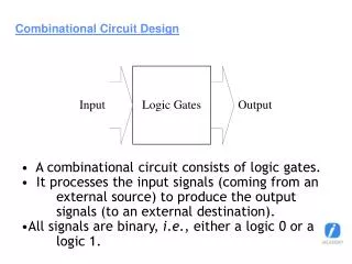
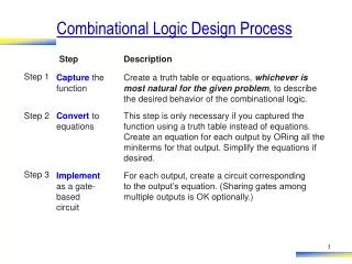
Combinational Circuit Design • The three main steps in designing a single-output combinational switching circuit are: • Find a switching function that specifies the desired behavior of the circuit. • Find a simplified algebraic expression for the function. • Realize the simplified function using available logic elements. 311_04
Example 1 F B A Define a two-valued variable to indicate whether each phrase is true or false: F = 1 if “Mary watches TV” is true; otherwise F = 0. A = 1 if “it is Monday night” is true; otherwise A = 0. B = 1 if “she has finished her homework” is true; otherwise B = 0. Because F is “true” if A and B are both “true”, we can represent the sentence by F = A • B 311_04
Example 2 • The alarm will ring iff the alarm switch is turned on and the door is not closed, or it is after 6 P.M. and the window is not closed. 311_04
Minterms and Maxterms 311_04
Minterm Expansion Find the minterm expansion of f(a,b,c,d) = a'(b' + d) + acd' 311_04
Design Example • Design an adder which adds two 2-bit binary numbers to give a 3-bit binary sum. 311_04
Truth Table 311_04
Incompletely Specified Functions don't-cares 311_04
Design Example • Design a circuit so that the output (Z) is 1 iff the decimal number represented in BCD is exactly divisible by 3. 311_04
Binary Adder Design 311_04
Binary Addition (Full Adder) 311_04
Binary Subtracter 311_04
Summary • Word Problems • Truth Tables • Minterms and Maxterms • Don't Cares 311_04